 NFM
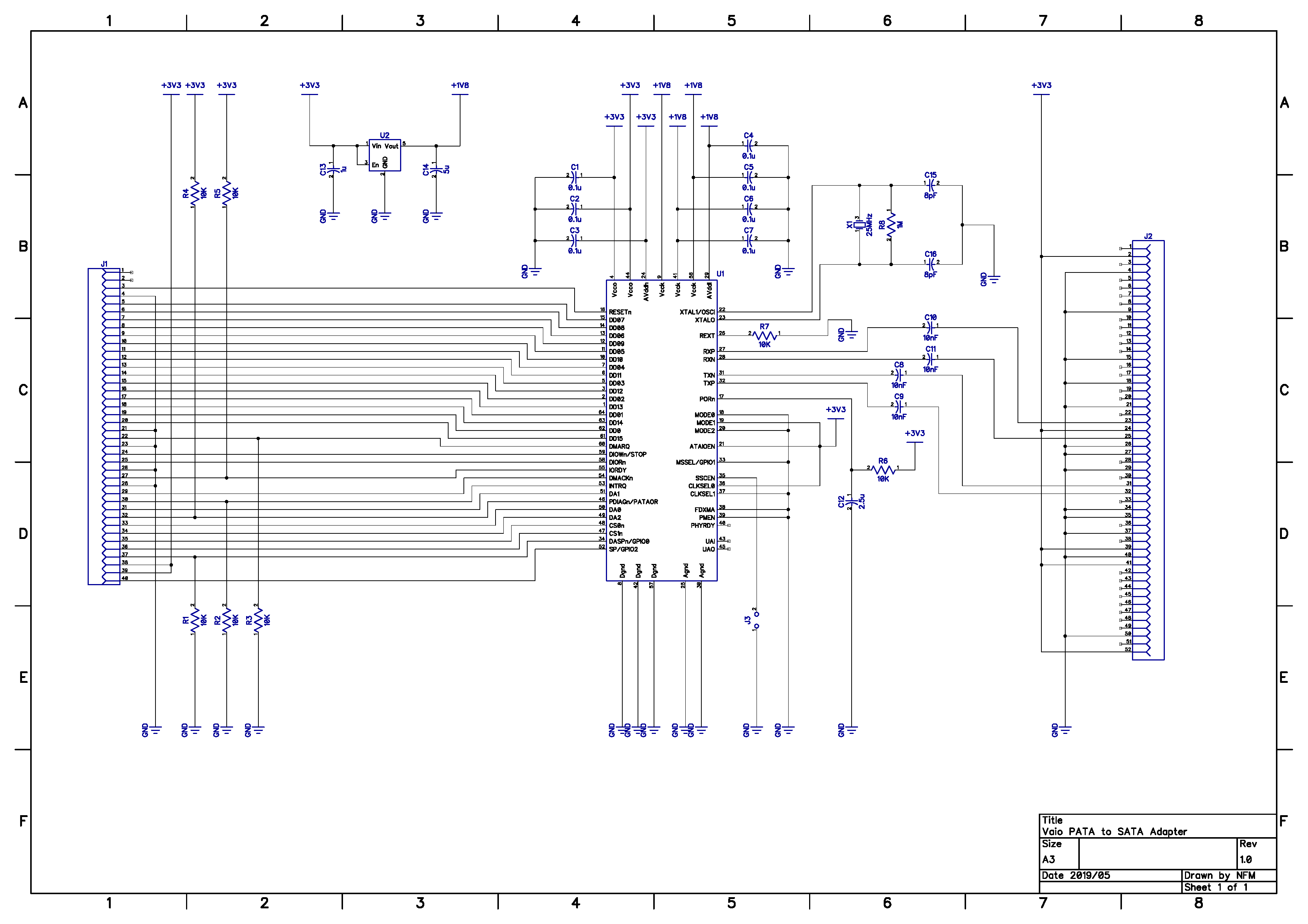
NFMI've been recently working on the schematic for the PATA to SATA adapter. (PATA on the left, SATA on the right).
It seems to be all sorted now, pending the small corrections I inevitably find later (hopefully before I spin the boards...)
I went a bit wild on the decoupling, just because, and at the bottom center-ish you'll see J3, this will be a solder jumper that can enable spread spectrum to reduce EMI if it doesn't affect performance too much (Benchmarks to see what happens later).
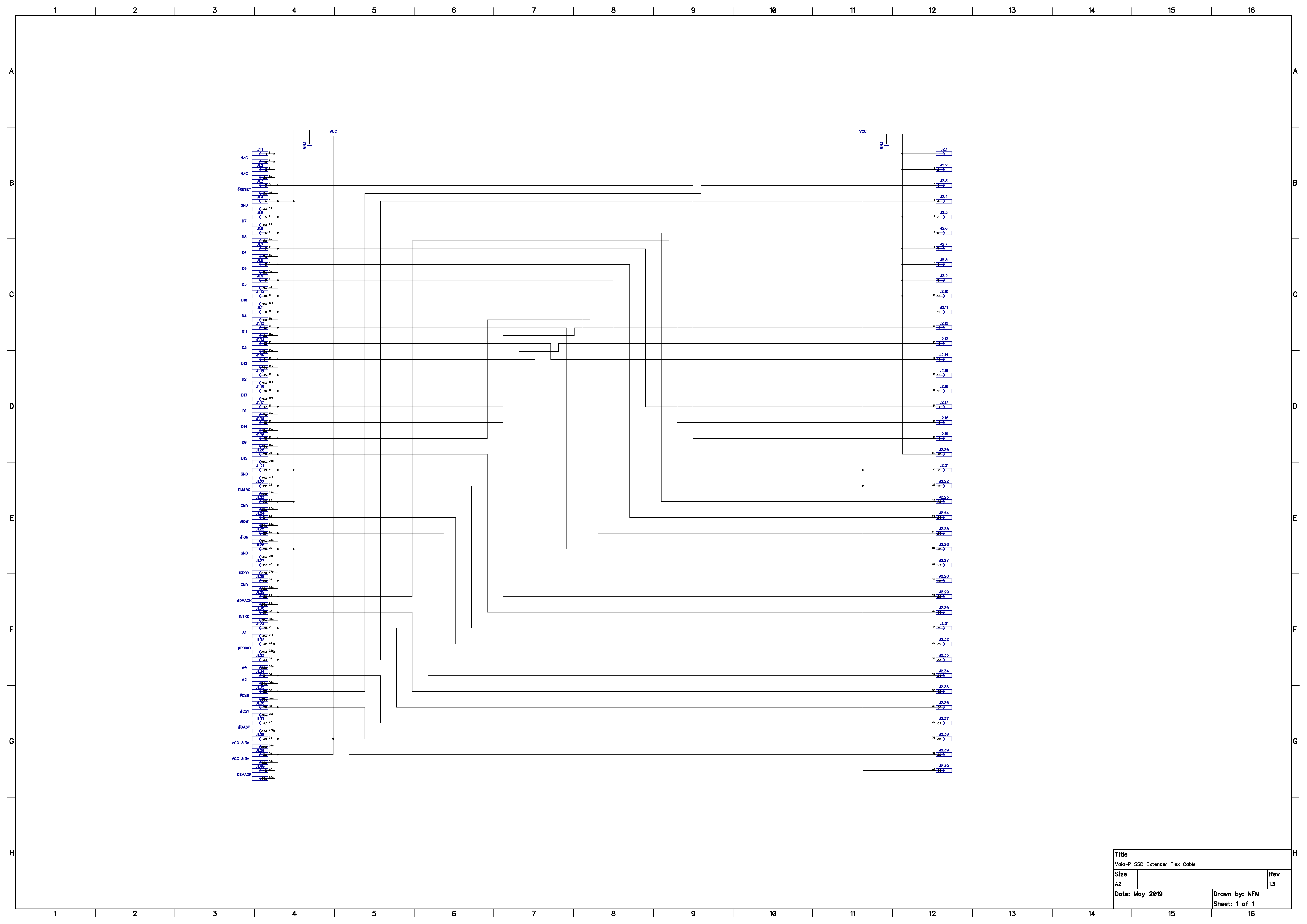
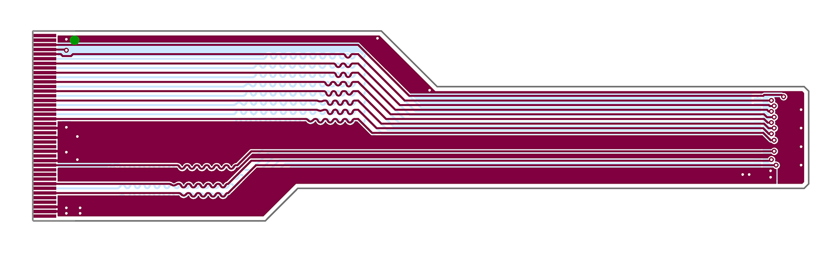
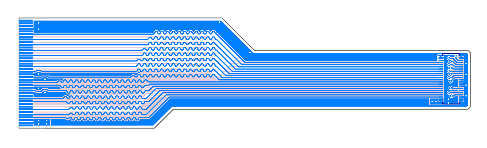
I also made a small revision to the flat-flex cable, I just moved that rogue connection to pin 40 up to pin 37 where it matches up as the indicator activity led as I thought.
I also tweaked the equal length traces to neaten them up a little too.
Discussions
Become a Hackaday.io Member
Create an account to leave a comment. Already have an account? Log In.