To design this project I used the great KiCad StepUp workbench, specifically the design flow from FreeCAD to KiCad using the outline exporter.
First I began on the part design workbench, by drawing a sketch on the XY plane, like so
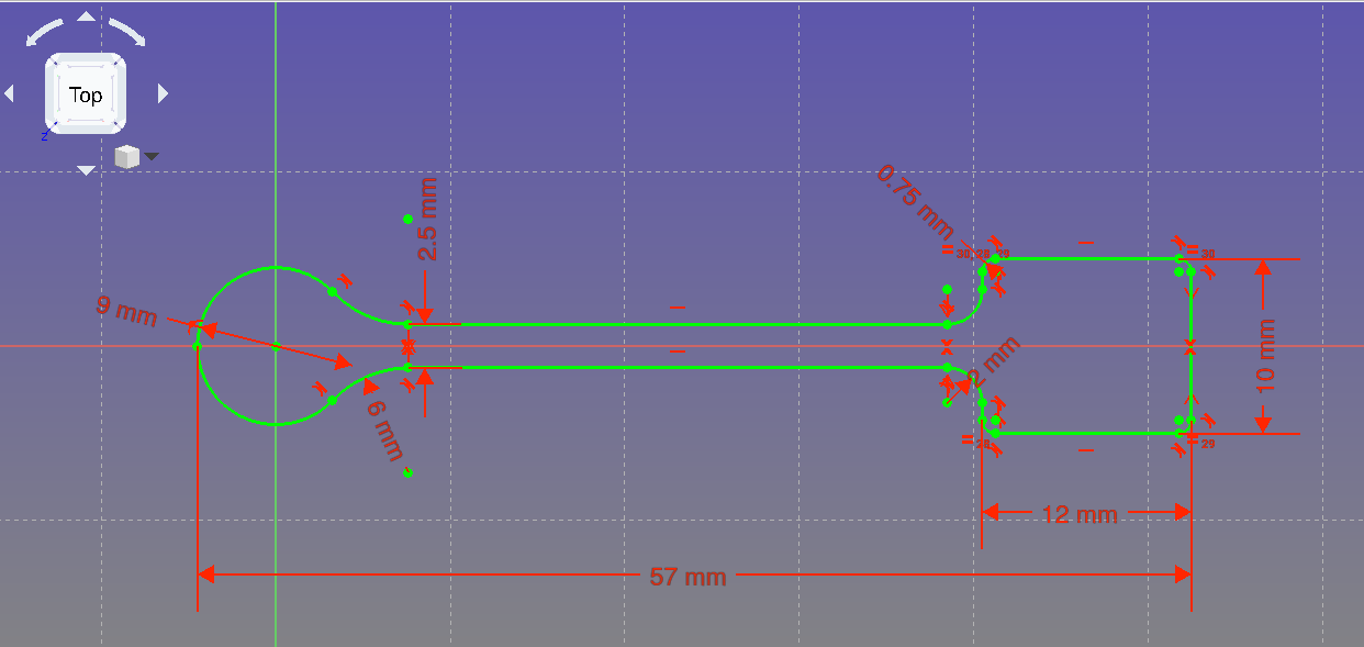
Once i was happy with my outline in FreeCAD I just switched to the KiCad StepUp workbench and pressed this button: "Push sketch to PCB edge"

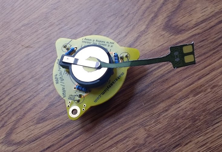
 Using planes eases the creation of a proper "Teardrop" into the round pad, without the smooth copper transition the copper foil would crack at that point on bending.
That is basically it... Will update when prototypes arrive.
 Jose Ignacio Romero