 Victor Dedios
Forget about yourself, capture user feelings
Sometimes, as hackers, engineers or designers, we fall in love with the most technical side of a
project getting to justify it from that perspective. But we forget that, when building things beyond
our own pleasure, technology is just a tool to solve that problem our customers have to face.
Which one scares you more?
Last log, I explained the main problem this project aims to solve which we could summarize in the difficulties we still find when prototyping PCB at affordable prices and in fast times. The solution would include a user experience with almost no interaction: out of the box use + load a design + press print. The idea is that the user can get an almost finished product, even solder paste dispense and component solder, with minimal interaction.
To get this, the PCB manufacturing platform should include at least this characteristics:
-
Minimal assembly when unboxing
-
Affordable: under 500usd
-
Fast: Less than 45 minute process
-
Professional end: Double sided layer, 0.1mm traces, drilling, cutting, solder mask, minimal silkscreen
-
Solder paste dispensing
-
Solder reflow
-
Auto-level
-
Auto tool changer
-
Protections: shutdown recovery, over voltage, lost step count and more
This list is open, it may change and it will be growing as the project moves along and new challenges are encountered. It is mostly illustrative and intended to show the main goal characteristics.
Ok, but what about the different technologies?
I ́ve done a lot of research of the main techniques used when prototyping PCBs and made this brief summary comparison table with the main ones:

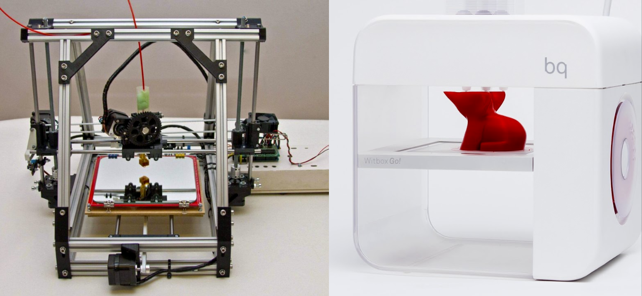
CNC + milling
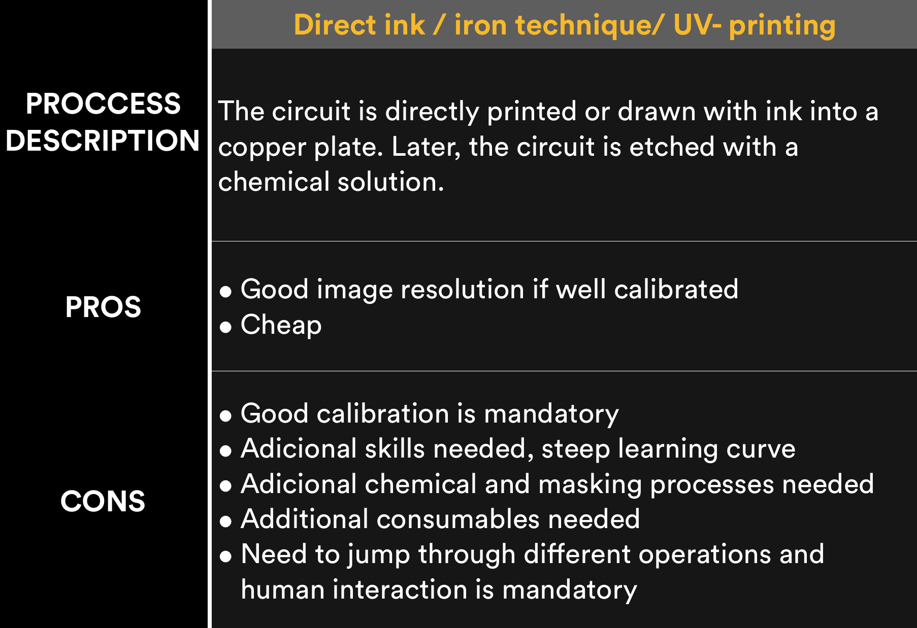
Direct ink/ iron/ uv printing
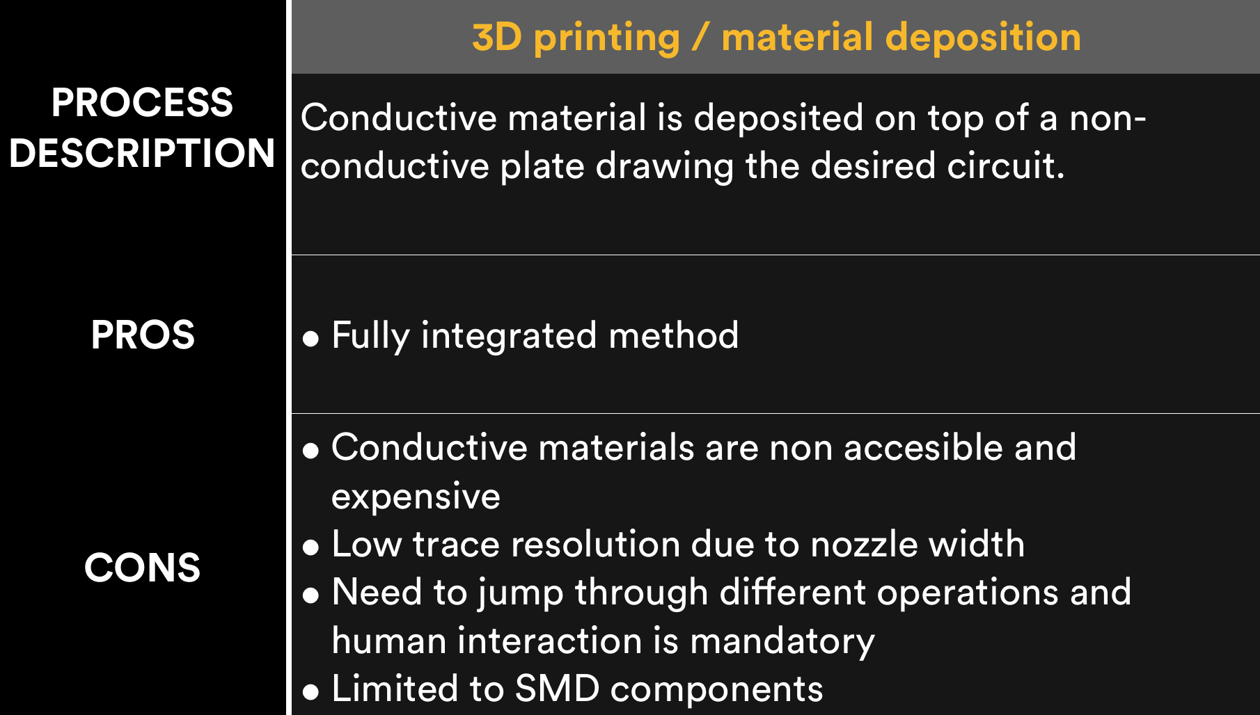
Conductive material deposition
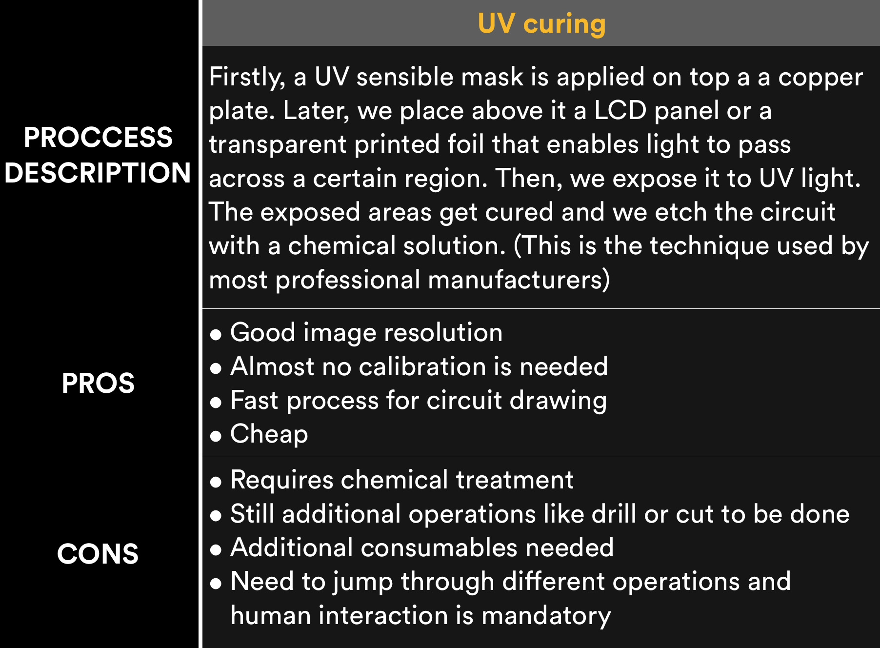
UV curing
Laser engraving
And what about the user?
Now that we know the main techniques as well as their main weaknesses/strengths, they are
compared from a user-perspective point of view, supposing that we want a fully ended PCB with
minimal human interaction. We have talked about the main user problems and minimal
characteristics, those get summarized in this main categories:
-
Full integrated process: most of manufacturing steps are automatic so user gets to interact as little as possible.
-
Accessible and open technology: Easy to find, replace and repare parts/consumables
-
Simple to use: Almost no additional knowledge needed to operate.
-
High-end definition: Good end meets minimal testing requirements
-
Affordable: under 500USD
-
Less than 45 minute process considering all steps involved to get a fully ended PCB: etching circuit, making holes, cutting board etc.
The following table establishes if the main techniques shown above comply or not with each category (*all the comparisons are made having in mind a user with no additional skills and considering average market technology) :
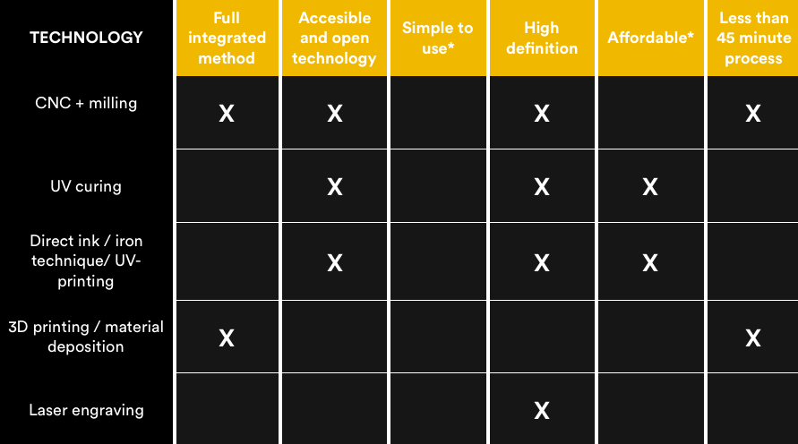
A decision has to be made
As we can observe, CNC+milling gets the highest score, 4/6. Nonetheless there are still two categories, “simple to use” and “affordable”, where it fails, although it still can be improved to meet the minimum requirements.
Having analyzed all the options and seeing the results, the main technology that will be used in this project is CNC+milling. This technology still has plenty of room for improving (even those categories where it failed ) which is what this project aims to solve. It allows to have a fully integrated process, is easy to replace and find parts, and, if well designed it could lead to low price, usage simplicity, speed an quality. CNC allows us, apart from milling and drilling, do additional tasks in a 3d environment like solder dispensing, picking and placing components and soldering.
Manufacturing process
The design process is "simple". A PCB is a bunch of traces forming the desired circuit, including holes for TH components and vias. After that, you have to cut the board into the desired shape, apply solder, place components and reflow everything.
This process will also include a solder mask option, but in a different way as usual. Instead of using a UV curable mask and a transparent sheet to expose it to light, we'll be directly starting the milling process with a fully masked copper board and milling away pad areas as well as the rest of the circuit. For this we will need a really well calibrated system.
Here you can see, the schematic process operation we would have with CNC technology:
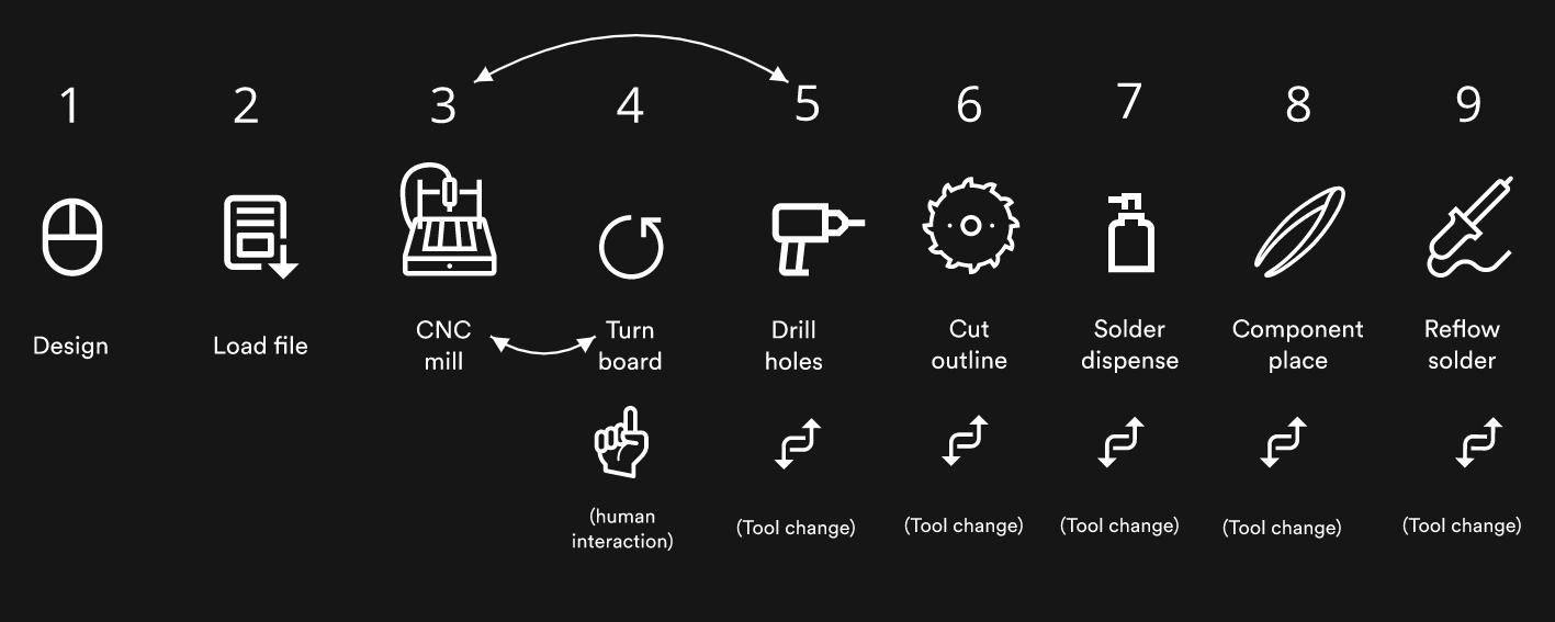
This manufacturing process is fully integrated, from a user perspective, you will get a complete functional prototype in a two step process
We observe that, with a fully integrated setup, there is minimal interaction from the user that could induce into an inaccurate operation or errors. This will also allow to operate the machine with no additional learning processes involved leading to a better user experience. CNC then gives us a good chance to design a process, like the one shown, to manufacture PCBs with almost only a single human interaction
That is all for now. Next log we’ll jump into designing and discussing the best mechanical model. Thanks and stay tuned!
Discussions
Become a Hackaday.io Member
Create an account to leave a comment. Already have an account? Log In.