This project aims to create a GPS antenna array with integrated amplifiers and RF switch on a flexible PCB for optimal GPS reception.
To make the experience fit your profile, pick a username and tell us what interests you.
We found and based on your interests.
GPS switcher.pdfPDF of SchematicAdobe Portable Document Format - 45.15 kB - 05/16/2019 at 05:36 |
|
|
GPS switcher.schEAGLE Schematicsch - 307.96 kB - 05/16/2019 at 05:35 |
|
|
GPS switcher.brdEAGLE Board Layoutbrd - 206.31 kB - 05/16/2019 at 05:28 |
|
|
I wasn't too happy with the original GPS chip antenna I chose for this board (1575AT43A40). It was really convenient though. It has a gain of -2.5 dBi and I was not too happy with the rf radiation pattern. (you can find the datasheet here: https://www.sparkfun.com/datasheets/GPS/JTI_Antenna-1575AT43A40_2006-09.pdf)
So I switched to a different ceramic chip antenna, the W3011A. This has a gain of +1.0 dBi and a return loss of -16 dB, which is much better than the -9.5 dB from the old antenna. In addtion, it doesn't need as much clear area around it, so I can make the board a little more narrow.
(datasheet here: https://www.mouser.com/datasheet/2/336/-13567.pdf)
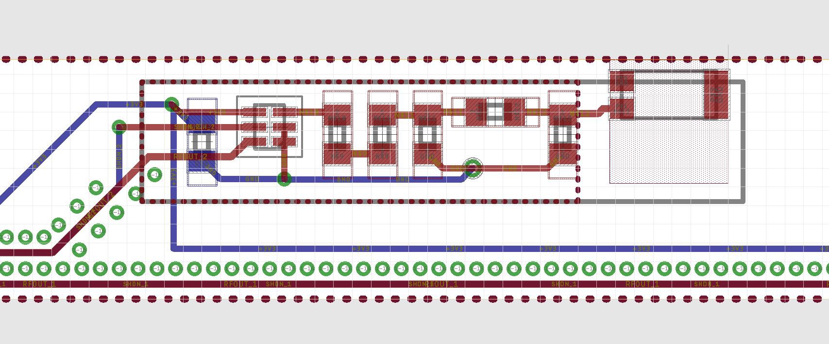
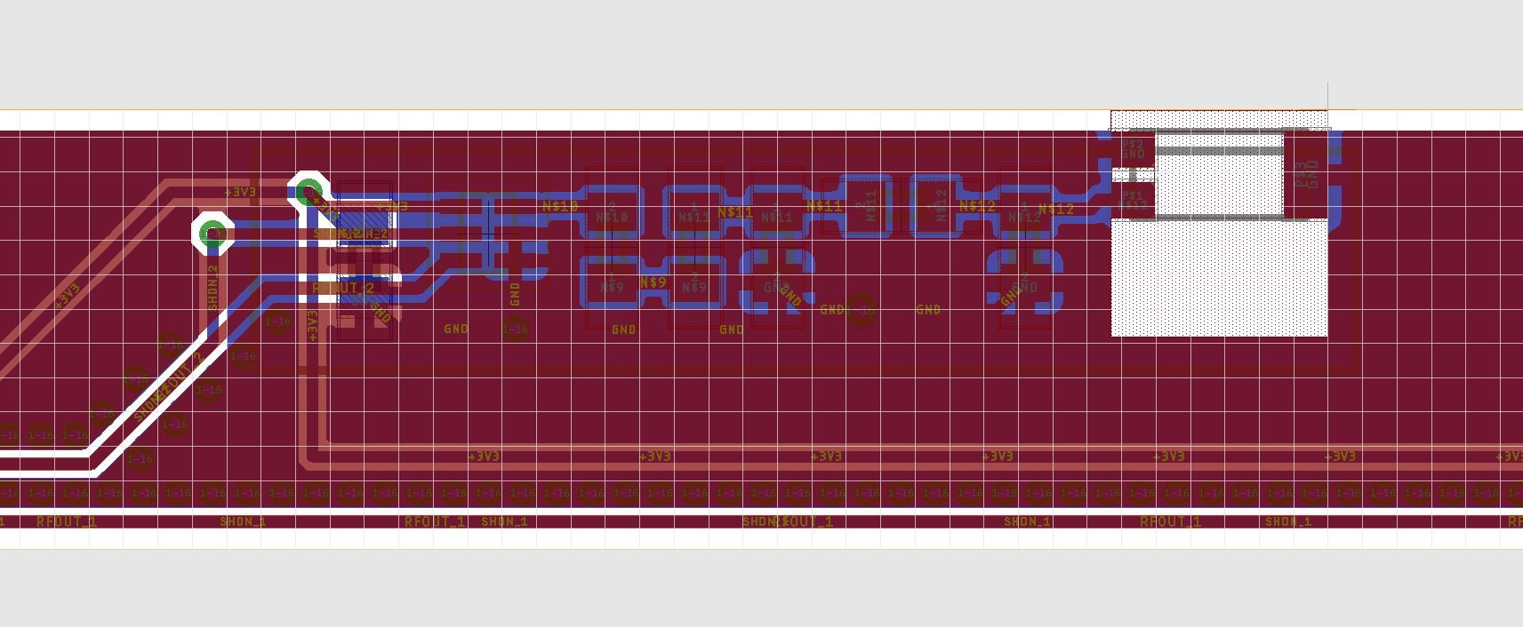
Also, here is a picture of the board layout for one of the 5 antennas + passives + LNAs. You can see the chip antenna in the upper right with the keepout layer to restrict the ground plane.
Create an account to leave a comment. Already have an account? Log In.
Become a member to follow this project and never miss any updates
By using our website and services, you expressly agree to the placement of our performance, functionality, and advertising cookies. Learn More