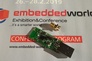
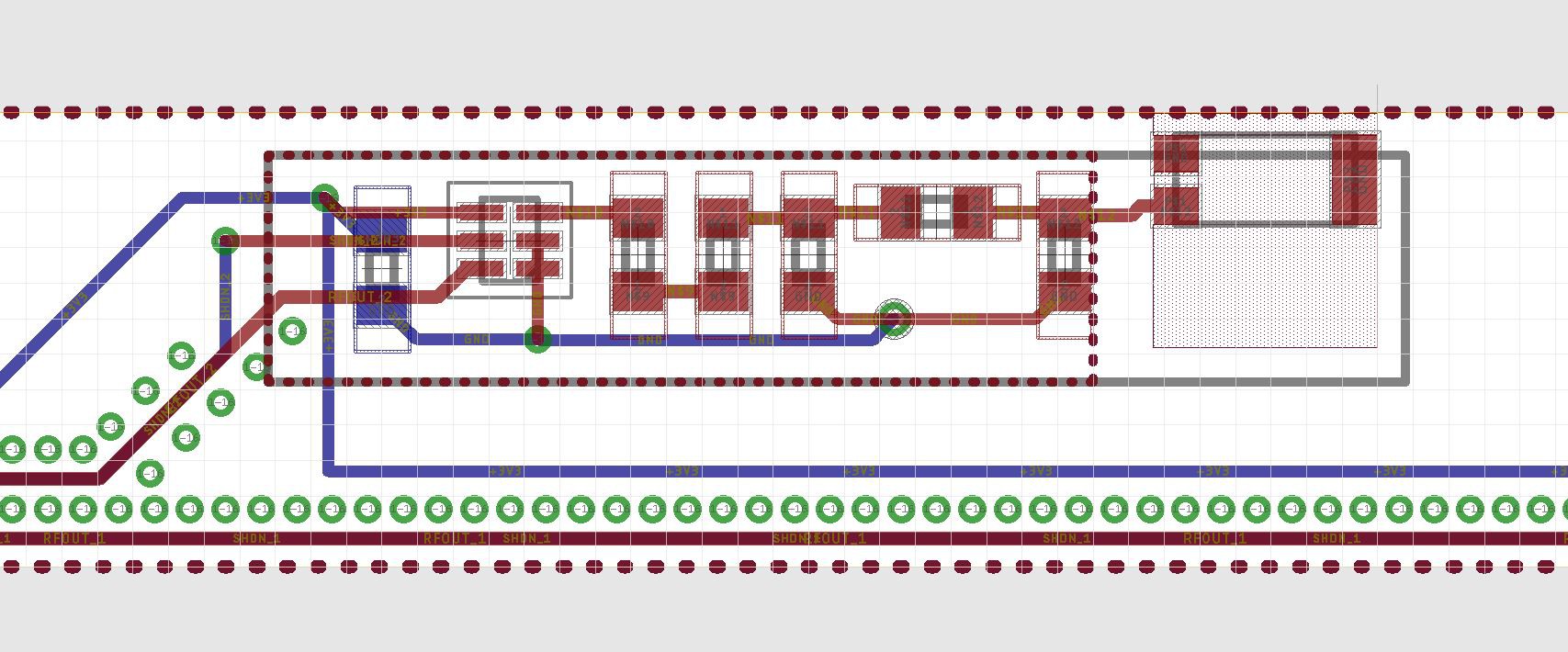
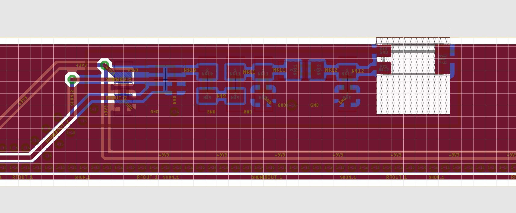
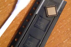
This project aims to create a GPS antenna array with integrated amplifiers and RF switch on a flexible PCB for optimal GPS reception.
To make the experience fit your profile, pick a username and tell us what interests you.
We found and based on your interests.
GPS switcher.pdfPDF of SchematicAdobe Portable Document Format - 45.15 kB - 05/16/2019 at 05:36 |
|
|
GPS switcher.schEAGLE Schematicsch - 307.96 kB - 05/16/2019 at 05:35 |
|
|
GPS switcher.brdEAGLE Board Layoutbrd - 206.31 kB - 05/16/2019 at 05:28 |
|
I wasn't too happy with the original GPS chip antenna I chose for this board (1575AT43A40). It was really convenient though. It has a gain of -2.5 dBi and I was not too happy with the rf radiation pattern. (you can find the datasheet here: https://www.sparkfun.com/datasheets/GPS/JTI_Antenna-1575AT43A40_2006-09.pdf)
So I switched to a different ceramic chip antenna, the W3011A. This has a gain of +1.0 dBi and a return loss of -16 dB, which is much better than the -9.5 dB from the old antenna. In addtion, it doesn't need as much clear area around it, so I can make the board a little more narrow.
(datasheet here: https://www.mouser.com/datasheet/2/336/-13567.pdf)
Also, here is a picture of the board layout for one of the 5 antennas + passives + LNAs. You can see the chip antenna in the upper right with the keepout layer to restrict the ground plane.
Create an account to leave a comment. Already have an account? Log In.
Become a member to follow this project and never miss any updates