 Mahesh Venkitachalam
I have written a blog article on the project here:
https://electronut.in/ice-bling-making-led-earrings-with-an-fpga/
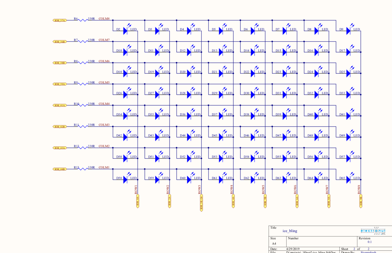
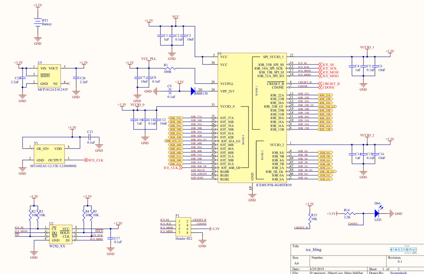
Here's the schematic for iCE Bling.
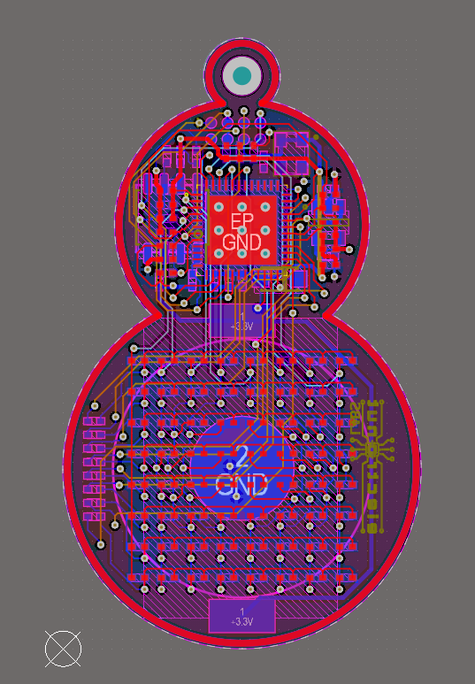
The PCB was designed using Altium Designer. It's a 4-layer board.
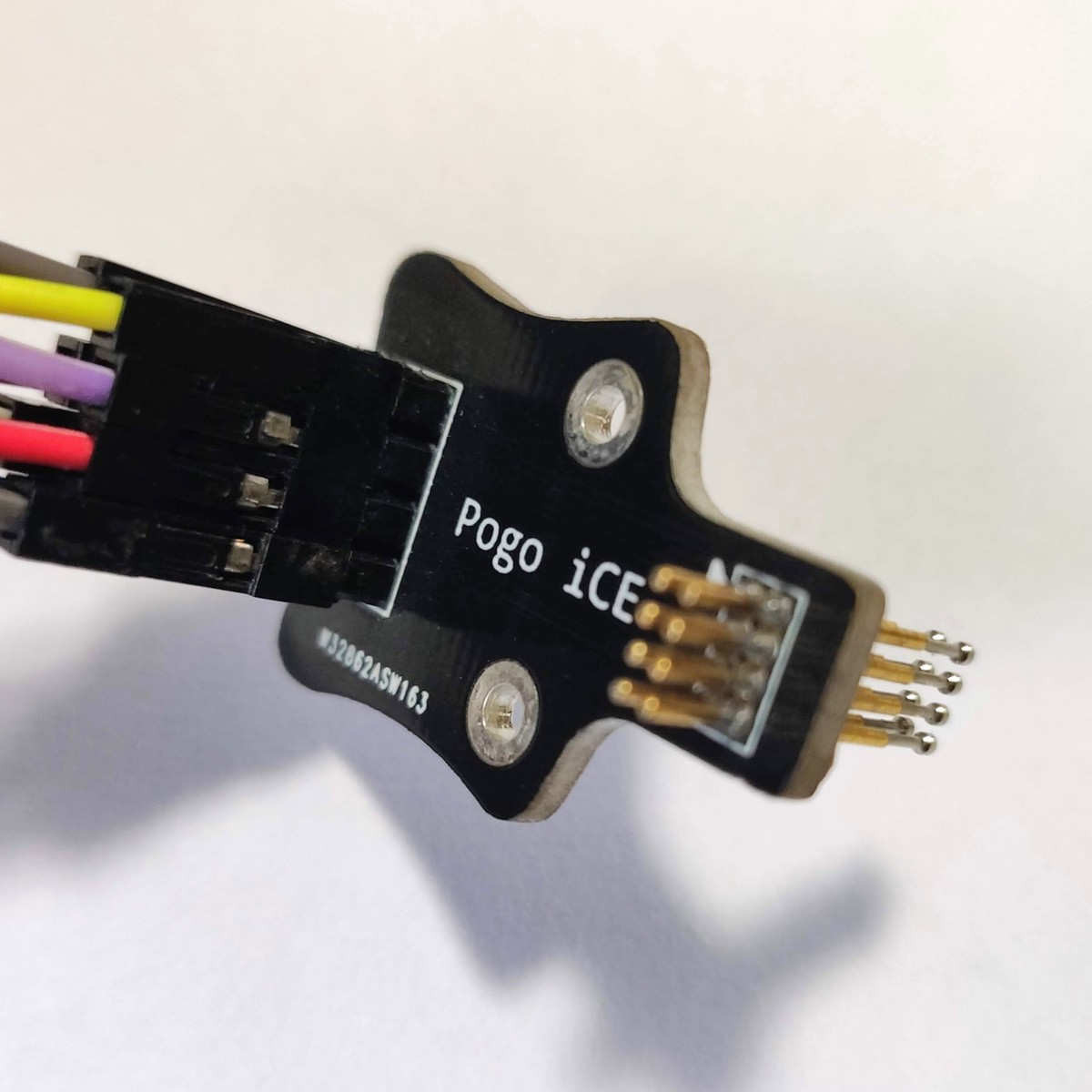
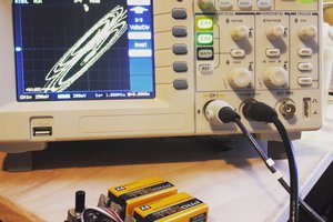
We also made a special pogo adapter for programming it:
Verilog code and PCB schematic (PDF) at repo below:
https://gitlab.com/electronutlabs-public/ice-bling
 Dylan Miracle
 Andrzej Strzała
 Supplyframe DesignLab
 Bhavesh Kakwani