Cees Meijer
-
The Power of Free
10/26/2020 at 20:16 • 1 commentWhile working on the Jupiter ACE project I was amazed, over and over again, by the power of the available free software tools.
![]()
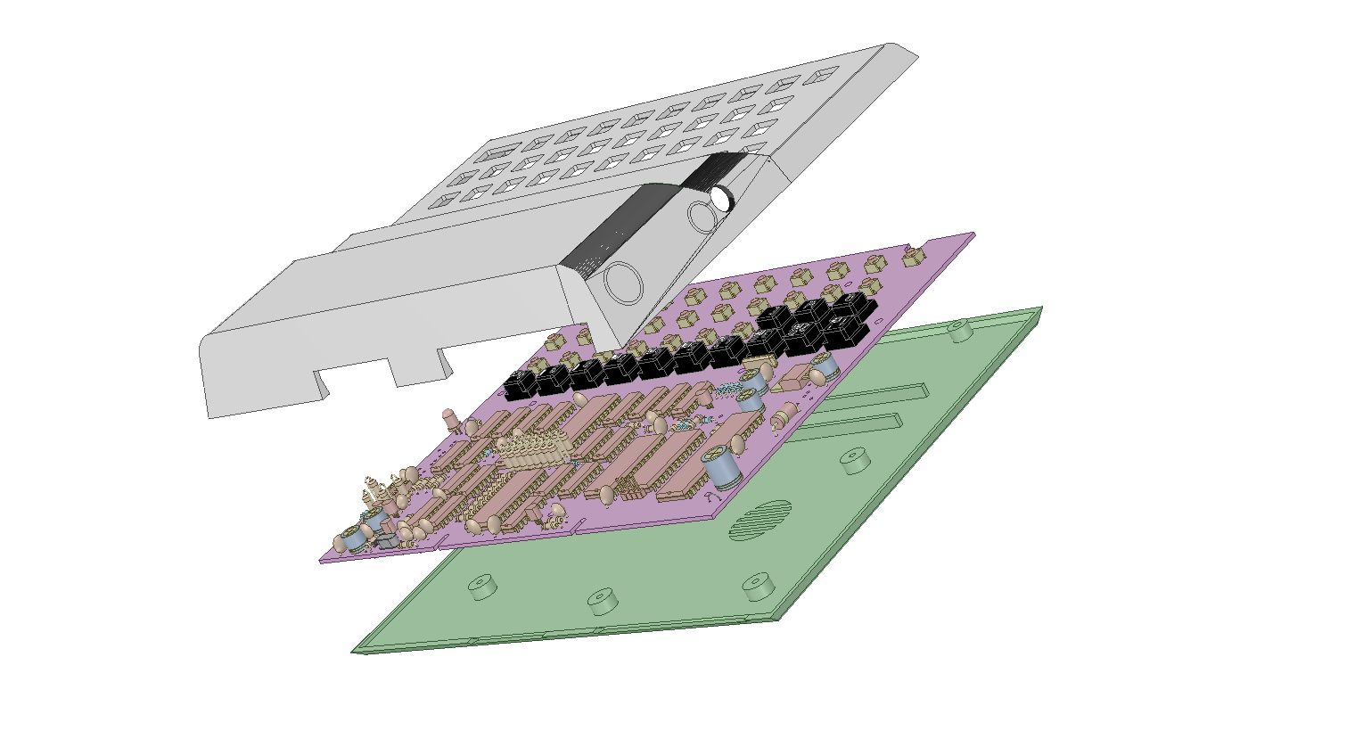
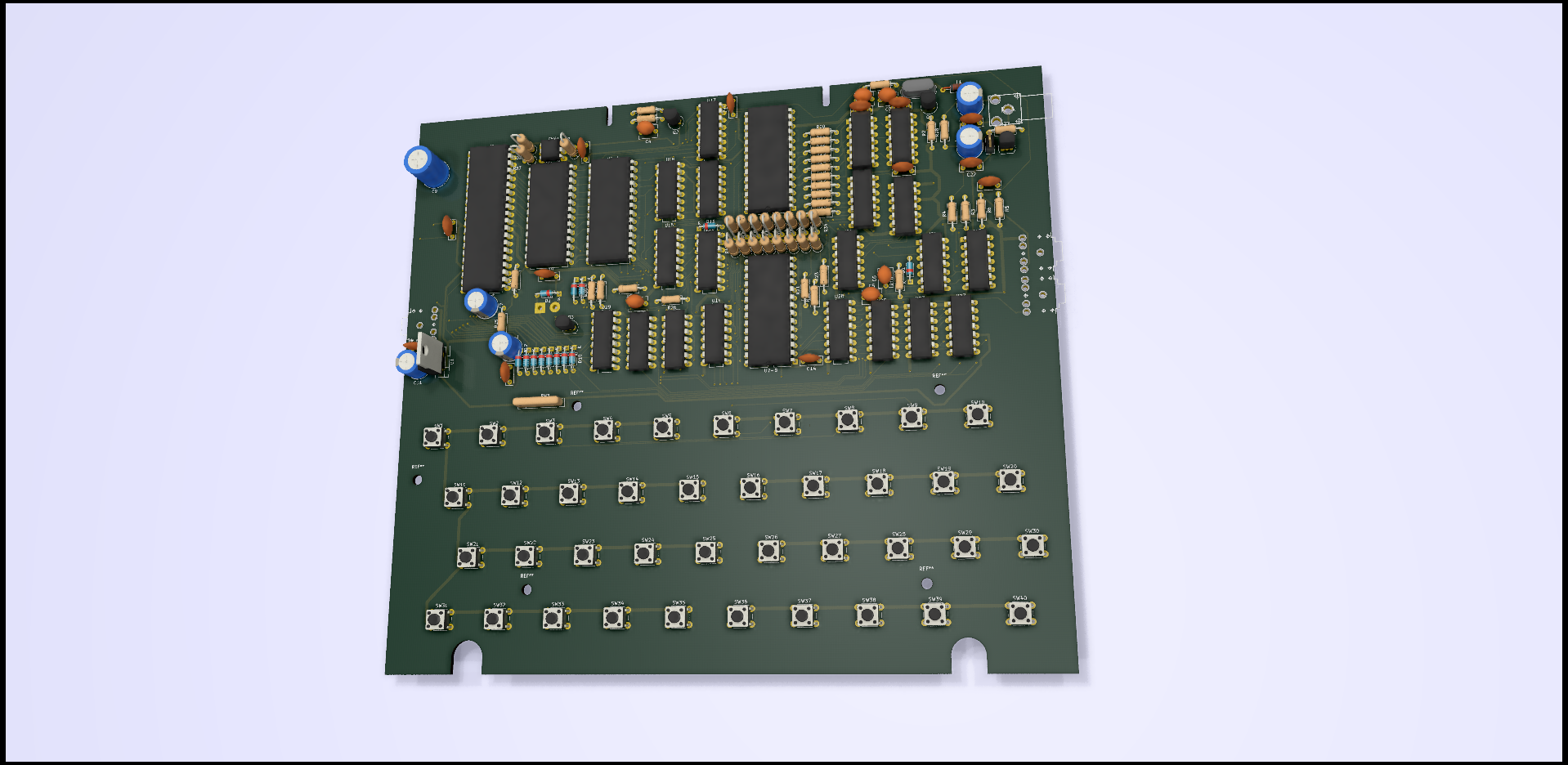
Housing drawn in DesignSpark, PCB imported from KiCad First there is DesignSpark Mechnical. An extremely powerful 3D CAD program from RS Components. It's a trimmed down version of SpaceClaim Engineer, a truly high-end CAD package. Which also means it misses some features, like directly placing texts, the option to mirror 3D objects, and the possibility to export to STEP files. Which sometimes makes makes it harder to get some things done, but usually there is a workaround. It does however support import of images or photo's. Which can be place and rotated in 3D space. Something that was tremendously helpful when drawing the Housing.
Second, of course, there is KiCAD. The free, open source, multi platform, Electronics Design package. With the release of version 5 it has really become a serious piece of software. It works flawless, and I've not seen it crash anywhere during my whole design process. The work flow has significantly improved since the previous version, and the available libraries are extensive. OK, you still cannot drag a component on your PCB while keeping the traces connected, but that's my only (minor) complaint. Tools like 3D view and STEP export on the other hand are truly amazing, and the only reason I could make an image as shown above.
And last, the PrusaSlicer. A fork of the (already pretty good) Slic3R. Since Prusa Printers forked it, and put a (full time) team of software engineers on it it has grown to be awesome. Adaptive layering, advanced move and align tools, customizable support, 3MF project support, its got it all.
![]()
-
Final Steps
10/17/2020 at 11:32 • 0 comments![]()
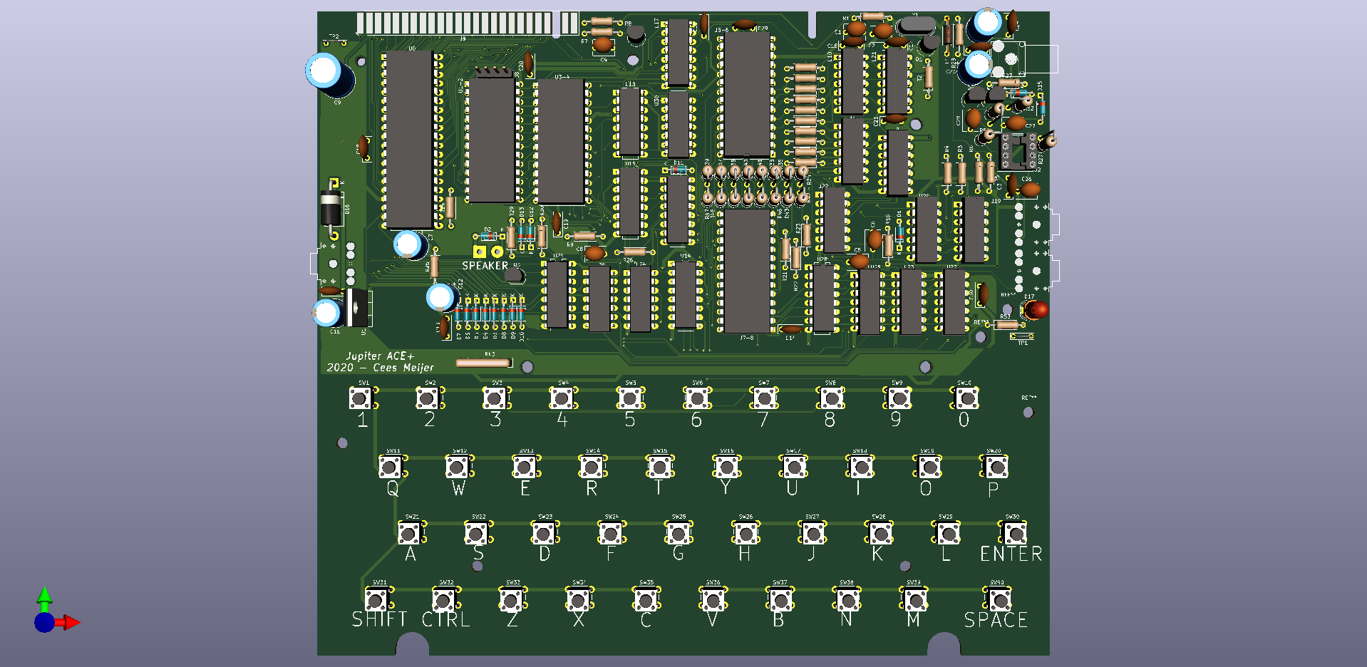
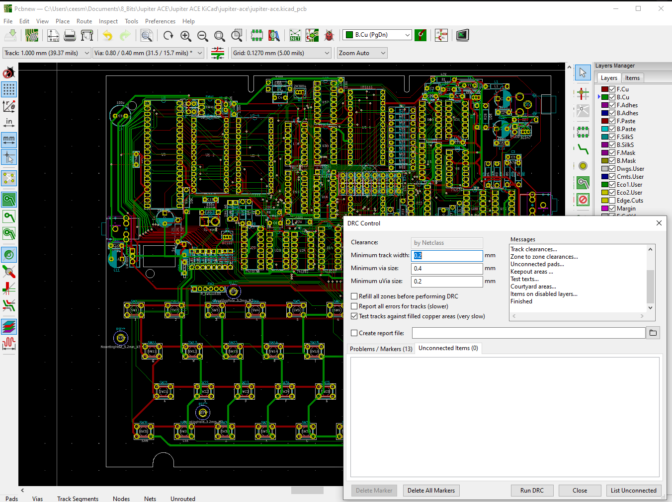
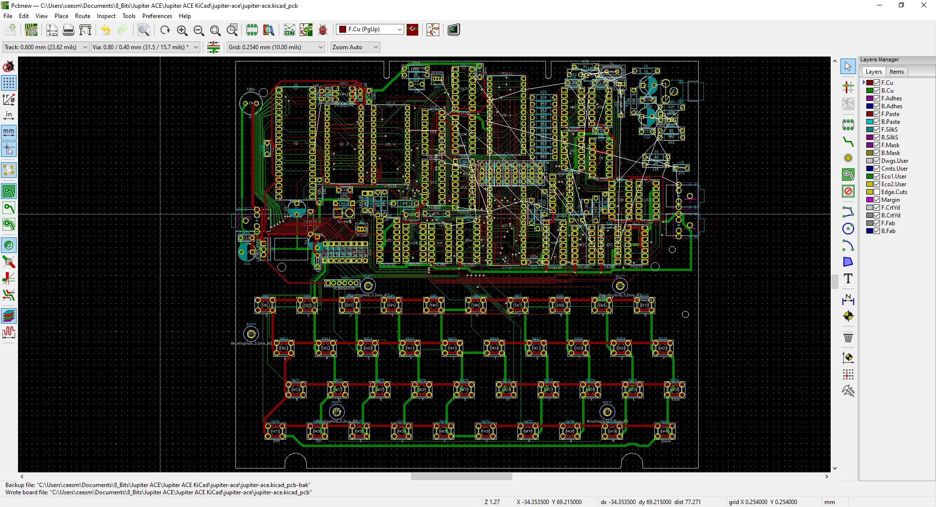
Now the routing is complete, and the moment where I have to send the design in for PCB production, it's time to go over the last details.
Decoupling capacitors
Someone mentioned that not all chips have a decoupling capacitor, and that could lead to problems. So I went over it and placed some extra 100nF wherever there was still space.
Silkscreen
Next, I added the letters / figures to the keys so they would be visible on the silkscreen. I first made all text in font-size 2x2, which seemed big enough on the screen. But when I printed the board 1:1, they appeared a bit small. So I found that the KiCad PCB file format is actually text, and that it was really simple to do a search / replace action to change the font size.
Footprints doublecheck
Checking the few footprints I was not sure of. Especially the transistors are notoriously difficult to get right. Countless are the boards where you have to mount the transistors backwards, on the bottom or worse: with two pins crossed. I also had my doubts about the 3.5 mm connectors for power and audio, but they matched perfectly on the paper printed layout,.
Zone fill for Vcc and GND
Added a few more 'zone fills' for VCC and GND. So far I routed all power lines using 1mm traces, but that is not much and could possibly cause problems with the (relatively) power hungry TLL chips. So adding a bit of copper here will definitely help.
Check the outlines
I found that I had two board outlines drawings. The first one was the one that I drawn by hand in KiCad itself on the Edge.cut layer, and the second one is the version that I imported from the mechanical drawing (which was more accurate) on the 'Dwgs.user' layer. So I removed all lines from the 'Edge.Cut' layer, and moved all relevant lines from the Dwgs.user layer to Edge.cut.
Add Diode and LED
As someone mentioned that the power plug polarity on the Jupiter ACE is different from that on the ZX80/81, I suppose its a good idea to add a diode to the power line. And then, it's always good to have a LED on the board so you can immediately see if the power is actually present.
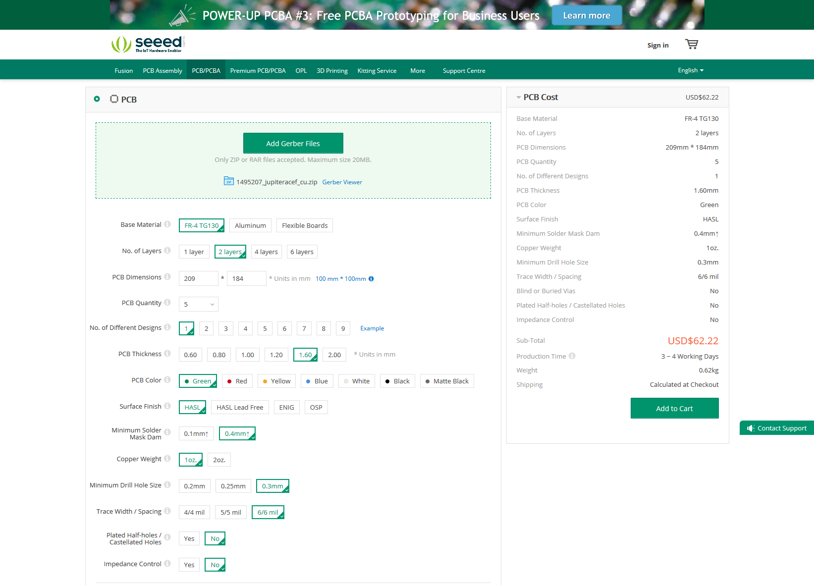
So, finally, I think it's time to send it to China, and have some boards made. I chose Seeed Studio for that. I've used them a few times before, and the boards are always very nice. The whole process of sending the files and placing the order is described on their site, and it is super simple. And they have their own Gerber viewer, so you can quickly see exactly what the boards will look like.![]()
US$62 for 5 pcs. Not too bad. Unfortunately the shipment will be another US$23, so the total will be around US$85,- Still not too bad. Let's hope the board is 100%, and I might be able to sell the extra boards... -
The Backporch
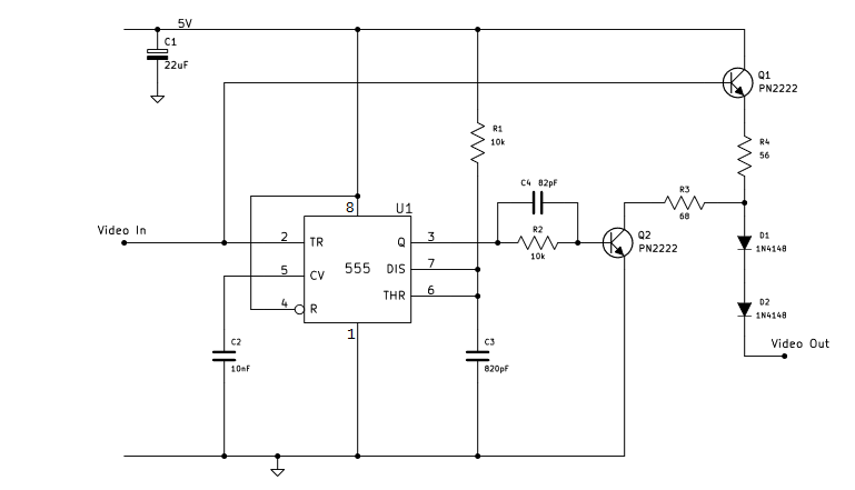
10/15/2020 at 18:56 • 0 commentsSomething that was pointed out to me in the comments by danjovic is that the video signal of the original ACE would probably need some additional conditioning. The signale misses something that is called 'backporch', which is essentially a short period following the sync pulse where the signal level is exacly 0V. The details are explained and shown in this nice video.
It's something that is also often mentioned regarding the ZX8/81 and Spectrum and therefore there are many circuit designs available that solve this. The one I liked most is the one which is also referred to in the video. It uses a NE555 chip, which seems sufficiently retro to me.
![]()
© Copyright 2015 Ziggurat Communications Ltd. (The document where I took this from says it could be freely copied, as long as it contains the copyright message)
So I will add this to my schematic as well.
-
What ? It already exists ??
10/12/2020 at 09:39 • 0 commentsJust as I'm finishing my PCB, and started looking for details on the one missing part (the edge connector), I found this forum:
https://forum.tlienhard.com/phpBB3/viewtopic.php?f=15&t=3207
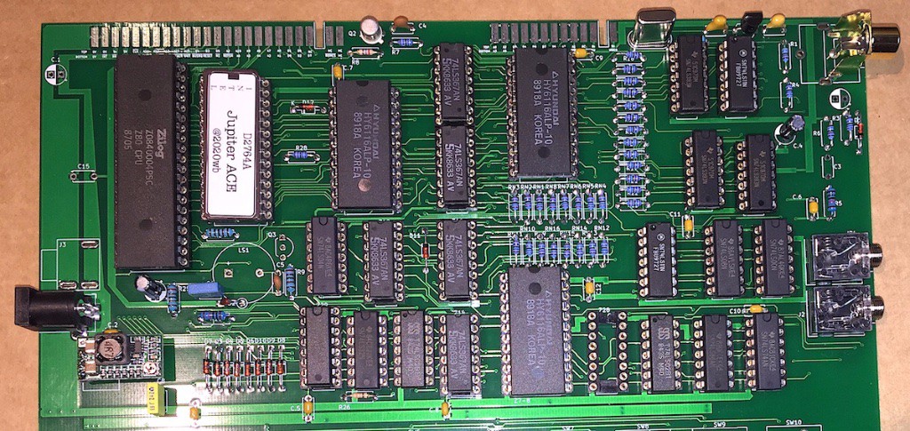
With images like this:
![]()
and this:
![]()
Yes, they look very, very similar to what I'm doing. So how is it possible that all the time I was researching for my project I did not bump into this site before ? It could be due to the fact that it is German site, and it is (partially) in German, but still. The actual board was made by 'rune' who's actually from the UK so all his posts are in English. Apparently a project that is only on a forum does not get a very high ranking on Google.
Digging through the forum, I eventually found the Schematic, layouts and BOM on this page. All very familiar. Now I have not (yet) engaged with this forum, but it looks like they have indeed been doing just about the same as me, over a similar timespan (2019-2020).
-
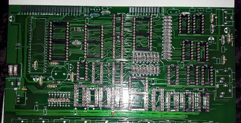
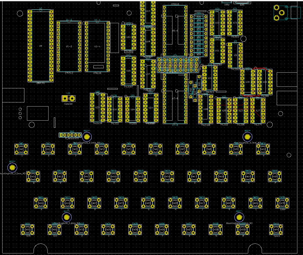
Routing Complete !
10/11/2020 at 20:34 • 0 comments![]()
Wait a minute !. Does it really say 0 (ZERO) unconnected ? YES ! It's been more than a year since I started this, and at least 2 times I considered giving up. But finally I completed the routing of the PCB !
Still have to go inspect it carefully (I actually spotted one chip that was not connected to power today...) but it looks like there may be an end to this project after all.
Oh, and I have not yet added the edge connectors :-( These are not supported as standard components by KiCad and so I'll have to make them manually. Which is probably going to take some time as well.
![]()
(This 3D view in KiCad is such an awesome feature)
-
Slowly, but still making progress
10/11/2020 at 10:38 • 0 comments![]()
As mentioned before: the routing is getting harder and harder... A few months ago I nearly gave up as it sometimes took me a full evening to get even a single track routed. But after focussing on some other projects for a while I decided to give it another try. And it's still hard, but it looks like I'm finally getting there. Just another few weeks to go...
-
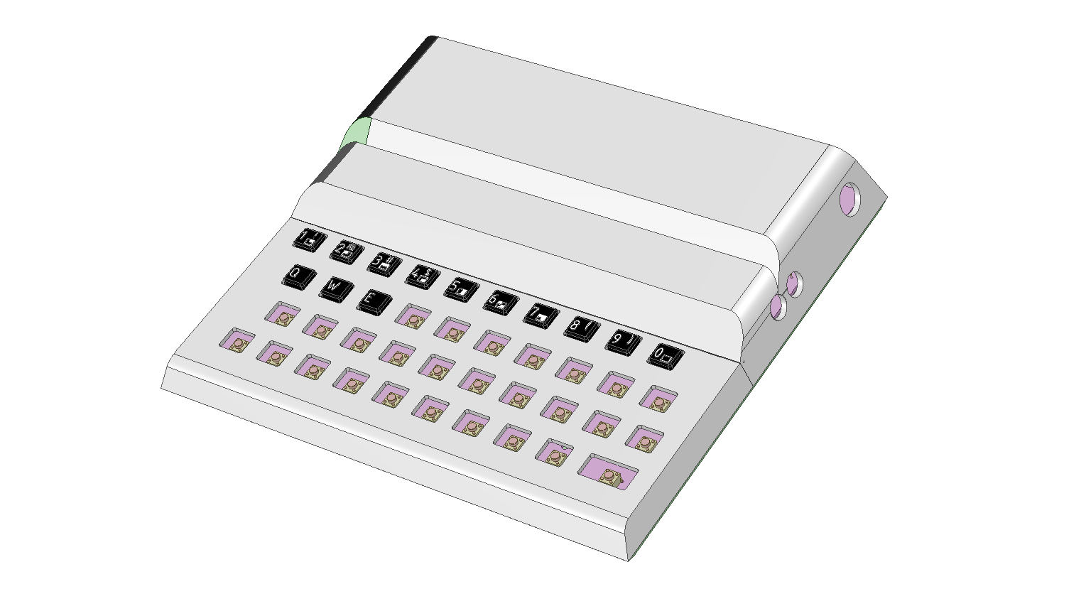
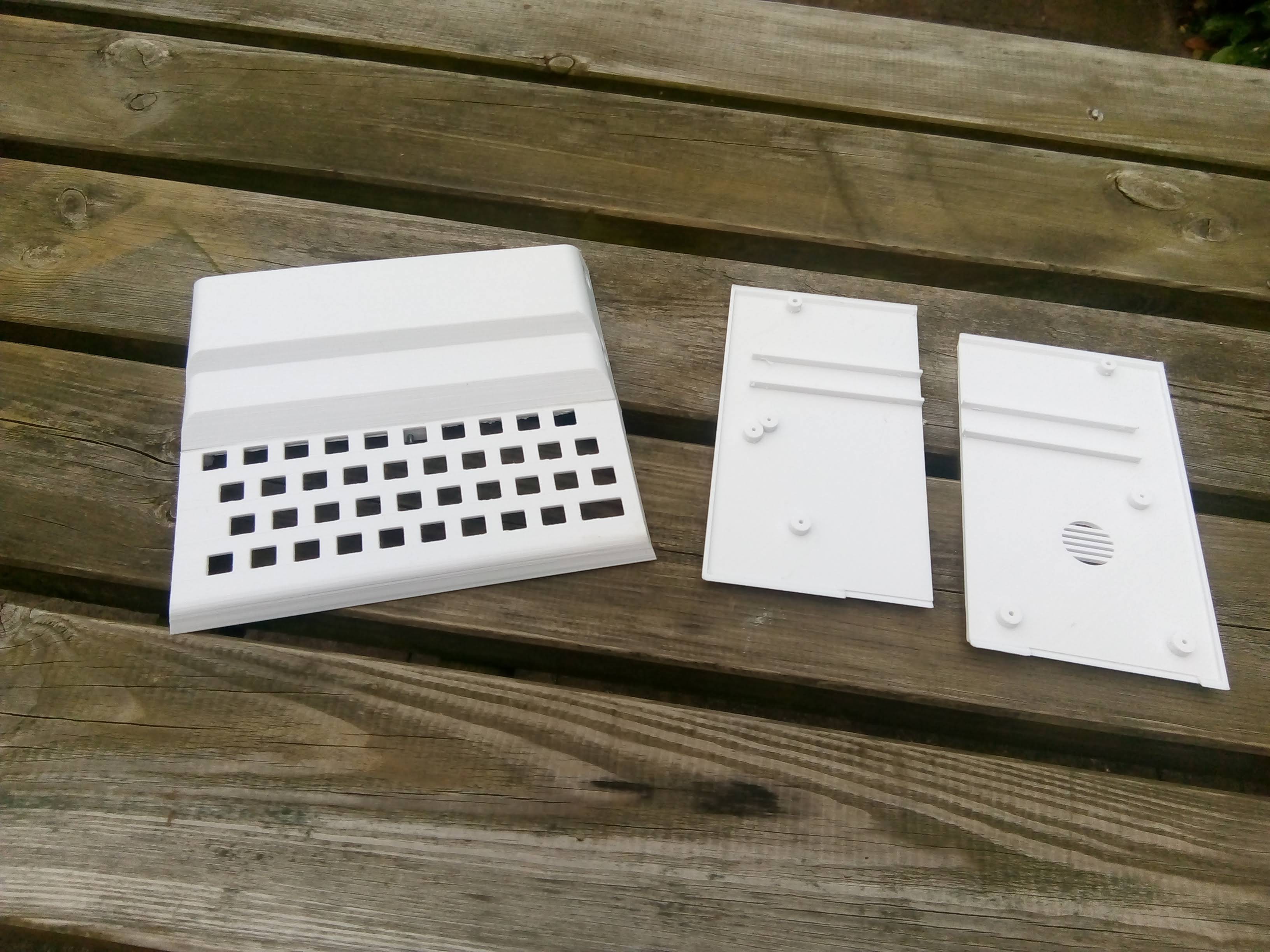
Housing
03/31/2020 at 14:53 • 0 commentsAs I'm still struggling with the PCB, I thought it was a good time to finish the housing. This worked out very nice. Printed both the top and bottom in two sections.
![]()
-
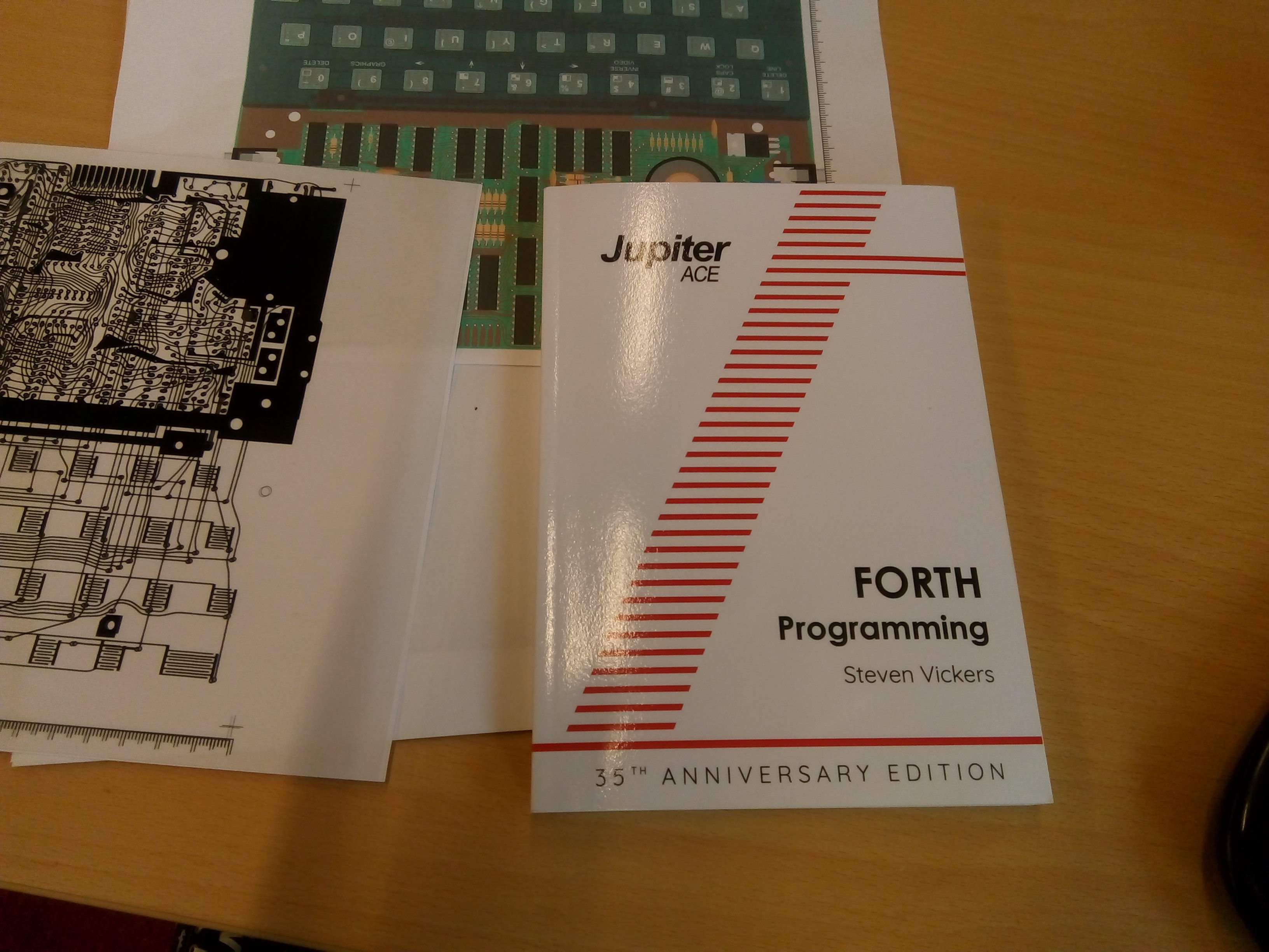
Progress, and a manual
08/29/2019 at 20:09 • 2 commentsRouting is progressing, but not as fast as I would hope. Originally I thought that I could simply follow 90% of the routing on the original board. But since there are a few major changes, like the type of RAM and the addition of some components for video and power supply decoupling, this soon became impossible.
![]()
A lot of routing is done, but as the ratsnest shows, the best is yet to come. So I decide to let that go, and just route as I (and the Kicad router) think is best. Which still means a lot of work.
In the meantime I finally ordered the 'Jupiter ACE - FORTH programming' book by Steven Vickers.![]()
Very nice to have at least the original manual for my computer, even though this computer itself is still in the future. -
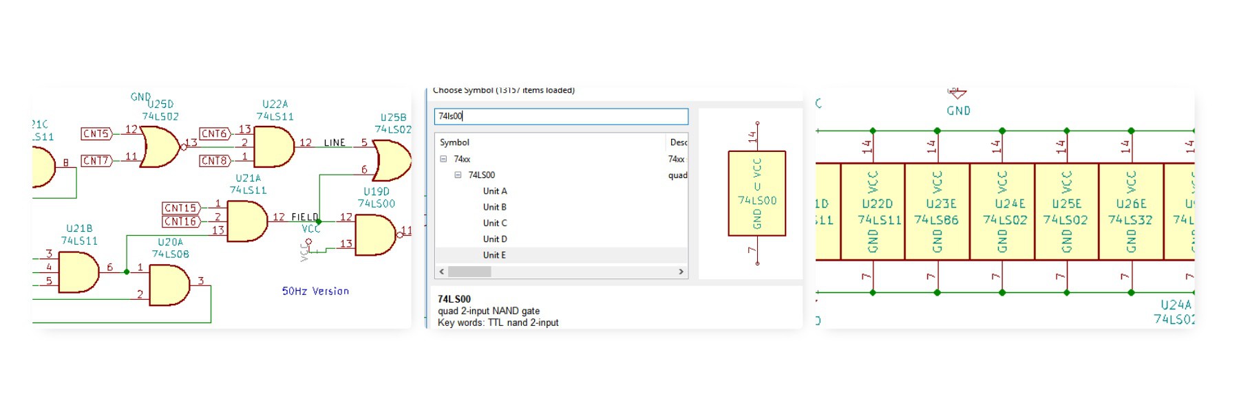
The Mystery of the Missing Power Pins in KiCad
06/27/2019 at 20:14 • 5 comments![]()
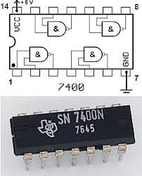
After I placed most of the ICs on the PCB, mostly according to the original layout, I started to try and route them. And by following the routes by looking at images of the original PCB it seemed quite simple. But when routing what looked like power and ground it suddenly struck me that two pins on both corners were connected. Since I have worked a lot with ICs of the 7400 series in the past I knew that most of them had Vcc and GND on two outer corner pins so this did not seem right.
![]()
7400 Power pins A closer look at the traces that connected the corners also showed that these did not have a net name. On the schematic there are also no power pins for any of the 74xx chips. But all Kicad guides that I could find also mentioned that power pins for logic chips are always hidden, and automatically connected to VCC and GND. There is a 'Show Hidden pins' button, but clicking it does not reveal any pin on a 74xx port. On the PCB it looks like all power and GND pins are simply connected by a net that has no name. This really puzzled me for while, until I discovered that all 74xx units actually have an extra unit that contains the power connections. So the 7400 contains 4 ports (Unit A,B,C,D) and a Unit E which only contains VCC and GND.
![]()
Ports, Unit E (power and gnd), and power ports in the schematic After adding the power 'unit' for every chip, the PCB routing suddenly makes sense and the pins are also marked with their correct names.
-
PCB Layout
06/15/2019 at 12:47 • 5 comments![]()
OMG ! How am I ever going to solve this ? After finishing the schematic, it's time to start the PCB layout. First this requires some decisions on what component shapes to use. All the ICs are easy, these are just standard DIP packages. The capacitors are all ceramic discs, but with a 5mm pitch, where 2.54 is more common these days. Resistors are all good, old-fashioned standards 0.25 W radials with a 10 mm pitch.
For the 3.5 mm jacks that connect the power and the tape recorder I chose a model that's available at almost every electronics shop. (Sparkfun sells it as '3.5 mm Audio Jack'). And for the RF or Video out a very standard RCA jack will do
(UPDATE 2020: The RCA jack in the image is actually obsolete. Something I only noticed after ordering my PCB. And surprise: it's also a model and pin-out that is extremely uncommon... )

RCA Jack, switches and 3.5mm Audio jack
And finally the switches, which I already decided to be the the 'mini tactile switch, 6x6x5'.
Recreating the Jupiter Ace
Recreation of the 'Fastest computer in the Universe' that runs FORTH.