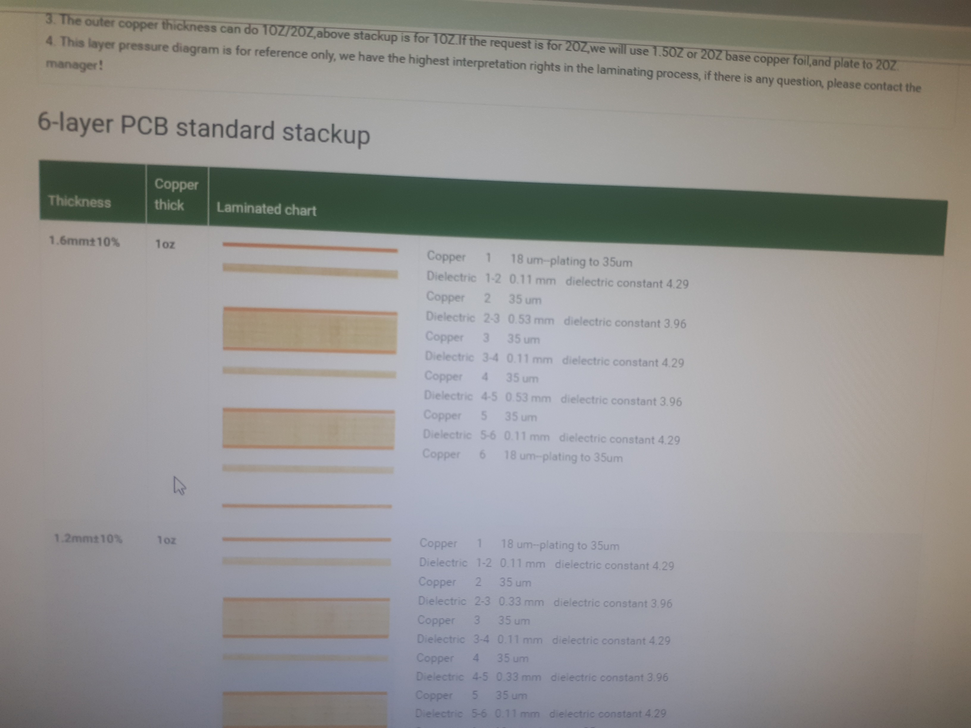
One of the final steps before finish the board is setting up the design rules for the PCB, most of the rules are defined since the schematic capture but this one is very important to match the proper impedance to the RF tracks. I need to define the stack structure for the PCB and I going to use the 6 layer standard stack of the manufacturer to make easy (and cheaper) the process.

 Raúl Luna
Discussions
Become a Hackaday.io Member
Create an account to leave a comment. Already have an account? Log In.