We know you have a lot of projects to get through, so we’ve put together this brief on our project as it pertains to the criteria of the Hackaday Prize.
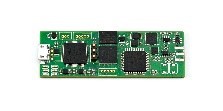
First of all, what is the Probe-Scope? It’s an open-source oscilloscope running at 250Msps with 60MHz of bandwidth, in the form factor of a cable; imagine you cut the BNC end off of an oscilloscope probe, and replaced it with a USB port: that’s the Probe-Scope.
i. Is this a unique solution to a particular challenge facing the world today?
The Probe-Scope is an innovation in the world of oscilloscopes, bridging the gap between the current low cost, low performance open-source oscilloscopes, and professional, expensive, closed-source oscilloscopes.
The Probe-Scope grows as you grow, giving you as many channels as you have USB ports; it’s almost infinitely expandable to tens (or more!) of channels. We are shooting for every channel to cost around $100, putting it on par or even cheaper than the commercial closed-source solutions out there today.
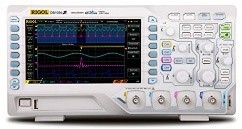
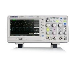
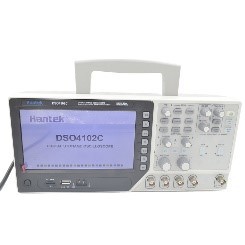
Closed-Source Comparison:
| Scope Model | Probe-Scope | RIGOL DS1054Z | Siglent SDS1052DL | Siglent SDS1202X-E | Hantek DSO4102C |
|---|---|---|---|---|---|
 |
 |
 |
 |
 |
|
| Price/channel | $100 | $88 | $130 | $180 | $145 |
| Open Source? | Yes! | No | No | No | No |
| Bandwidth | 60MHz | 50MHz | 50MHz | 200MHz | 100MHz |
| Voltage Range | 300V Pk-Pk | 300V RMS | 300V RMS | 300V RMS | 300V RMS |
| Memory Depth (Per Channel) | 16Mpts | 3Mpts | 16kpts | 7Mpts | 20kpts |
| Vertical resolution | 8 bits | 8 bits | 8 bits | 8 bits | 8 bits |
| Rise time | <5 ns | 7 ns | 7 ns | 1.8 ns | 3.5 ns |
Open-Source Comparison:
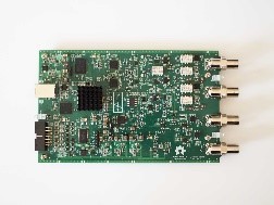
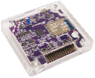
| Scope Model | Probe-Scope | Scope Fun | OpenScope MZ |
|---|---|---|---|
 |
 |
 |
|
| Price/channel | $100 | $375 | $75 |
| Open Source? | Yes! | Yes | Software Only |
| Bandwidth | 60MHz | 100MHz* | 2MHz |
| Voltage Range | 300V Pk-Pk | 40V Pk-Pk | 40V Pk-Pk |
| Memory Depth (Per Channel) | 16Mpts | 64Mpts | 32kpts |
| Vertical resolution | 8 bits | 10 bits | 12 bits |
| Rise time | <5 ns | 3.5 ns | 175 ns |
*The Scope Fun has no anti-aliasing filter and therefore can give misleading results
Clearly, there is a large market gap for a low-cost, high-performance open-source instrument. This is the gap that the Probe-Scope is designed to fit in.
ii. How thoroughly documented were the design process & design decisions?
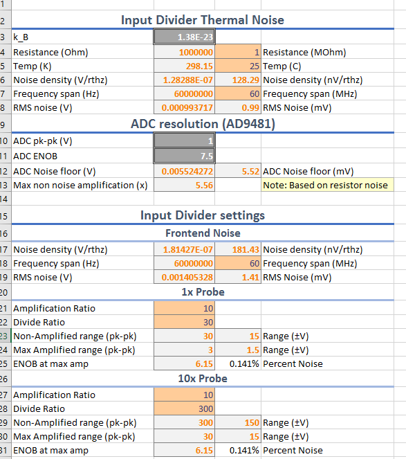
We have updates detailing every step of the design processes, everything from tricky design and analysis of high speed dividers to our process for laying out and assembling our boards.
We started with our detailed design and spreadsheets:
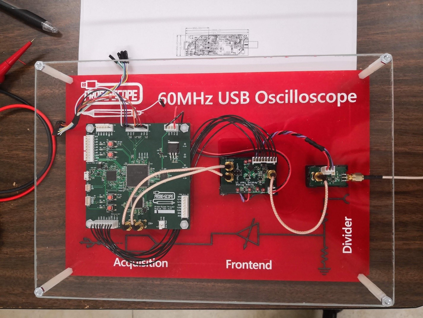
Then we moved on to a set of spread bench test PCBs to test all our subsystems:
And now we have our final PCBs hot off the press from PCBWay!
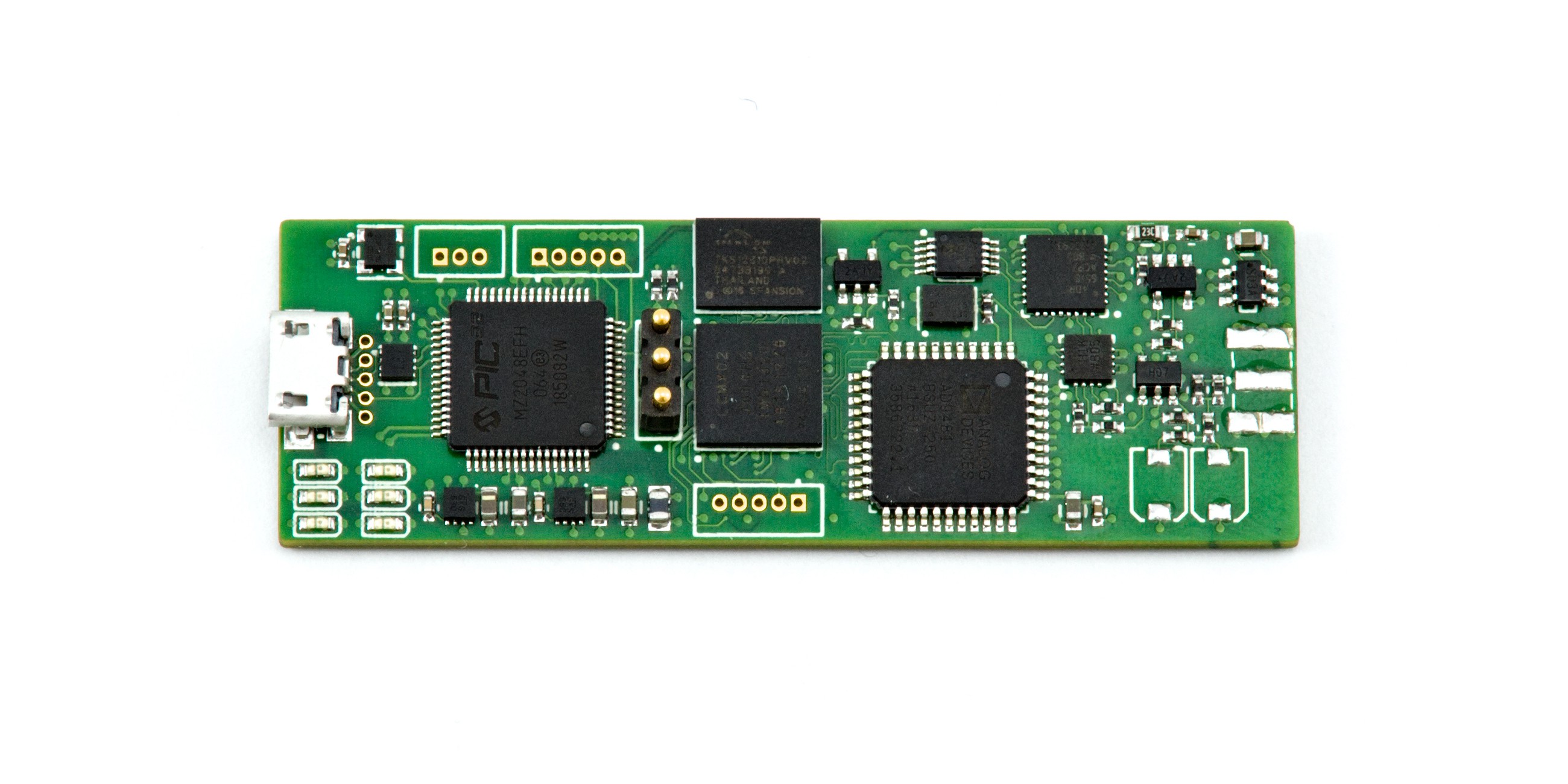
Here is a guide to all our updates:
- Introduction and Overview
- Analog Frontend:
- Digital Section:
- Final Design Bring up
Here is a guide to our GitHub Repos:
- Probe-Scope V1.0 PCB
- Embedded Software:
- PC Software
- Test Boards:
- Misc:
iii. How ready is this design be taken to market?
The hardware design is complete; our final PCBs were produced and assembled by PCBWay and functioned as expected right out of the box. We are planning on using the same design for volume manufacturing, with only minor changes to the connectors. The software is coming along nicely, more details on that in our next section.
iv. How complete is the project?
We have come a long way, having completing the following portions of the project in only 5 months:
- Market research, and viability
- Predesign
- Noise, Sensitivity and Bandwidth analysis (See our original calculations)
- Pre-BOM Pricing
- Feasibility and Form Factor
- Subsystems testing and development:
- Analog Frontend:
- Designing, building and testing Frontend Divider and VGA/Filtering PCBs
- Exceeding our initial bandwidth and noise specs
- Digital Board:
- Designing, building and testing the entire digital side of the system
- Testing all the components
- Providing an easy to debug test bench for Software Development
- Analog Frontend:
- Final PCB Production:
- Designing and Producing a very complex compact PCB
- High Speed, Length Matched busses
- 0.5mm BGA
- 6 Layer
- Blind/Buried Vias
- Via in Pad
- 3/3 Trace/Space
- Reducing total board area by 88% (18.8sqin to 2.2sqin) from our development boards
- Designing and Producing a very complex compact PCB
- Embedded Software
- PIC32MZ
- Created and implemented USB CDC protocol to transfer data. (See our protocol specification)
- Implemented USB CDC, SPI, I2C
- Implemented FPGA Interface for reading samples
- MachX02 FPGA
- Implemented sampling subsystem
- Implemented sampling FIFO
- Implemented PIC32 Interface
- PIC32MZ
- PC Software
- Implemented the USB CDC protocol
- Implemented capture, scaling and display of the ADC Data
- Implemented measurements subsystem (pk-pk RMS ect…)
From here this is our software roadmap:
- Expand current FPGA sample buffering subsystem to take advantage of the full HyperRAM (giving us 16M samples of memory)
- Implement trigger sharing on FPGAs
- Implement trigger delay on the FPGA
- Implement better (More “scope like”) horizontal and vertical scrolling on the PC software
- Implement many more measurements on the PC software
- Implement trigger sharing in the PC Software
- Change to dynamic Qt widgets to allow drag and drop rearranging of the capture display
We also have some stretch goals:
- Implement support for Sigrok decoders from the PC software to gain protocol decoding support
- Implement field firmware upgrades for the PIC32MZ and the FPGA (they are already hooked up just needs software)
- More things as we get more feedback!
 Mark Omo
Discussions
Become a Hackaday.io Member
Create an account to leave a comment. Already have an account? Log In.