We are adapting the circuit given by Tony Van Roon given in the book “Circuits for Hobbyists” (Page 75). This is an excellent book to start with if you want to do some tinkering with electronics
This project is sponsored by LCSC. I have been using electronic components from LCSC.com. LCSC has a strong commitment to offering a wide selection of genuine, high-quality electronic components at the best price. Sign up today and get $8 off on your first order.
Note: Generating Frequencies that could affect your FM band or any other communication band might be considered against the law in your country. Kindly use this circuit for education purpose only and make sure your signal is not too strong to disrupt any communication near you. For any mishaps neither the website nor the author can be held responsible.
The FM transmitter is a single transistor circuit. In the telecommunication, the frequency modulation (FM) transfers the information by varying the frequency of carrier wave according to the message signal. Generally, the FM transmitter uses VHF radio frequencies of 87.5 to 108.0 MHz to transmit & receive the FM signal. This transmitter accomplishes the most excellent range with less power.

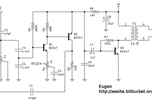
The following circuit diagram shows the FM transmitter circuit and the required electrical and electronic components for this circuit is the power supply of 9V, resistor, capacitor, trimmer capacitor, inductor, mic, transmitter, and antenna. Let us consider the microphone to understand the sound signals and inside the mic there is a presence of capacitive sensor. It produces according to the vibration to the change of air pressure and the AC signal.

In our circuit, the Audio Signal is given by a phone or iPod instead of a microphone. The Pre-Amplification is done using the LM386 Audio Amplifier IC. The 74LS138 along with 22 pf capacitor acts as a Tank circuit which produces a strong carrier frequency and modulate it with our amplified audio signal like the 0.1 uH inductor. We do not have a RF-Amplifier in our circuit, but it can be added if you need to achieve a higher range.

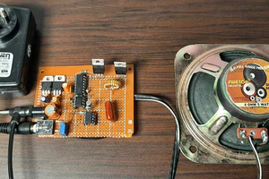
It can be built on a breadboard or soldered to a Perf board. The complete circuit can be powered using a 9 V Battery. If you are using an adaptor to power it make sure you add filter capacitor to reduce the noise from switching. The circuit uses an LM386 Audio amplifier which acts as an Pre-Amplifier, this IC amplified the audio signals from the audio device and feeds it to the Oscillating circuit.
The Oscillating circuit should have an Inductor and a Capacitor. In our project the IC 74LS13 which is a 4-Input NAND gate Schmitt Trigger is designed to oscillate at 3rd order Harmonics which is around 100 MHz. A filter capacitor across the power rails of the IC is very important to make it working.
The 3.5 mm Audio Jack has three terminals in which are for channel L, channel R and Ground. We short the channel pins so that it becomes mono channel as shown in picture below and connect it to pin 3 and ground is connected to pin 2 of LM386.
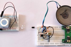
Thanks to the approach given by Tony Van Roon tuning this FM Transmitter circuit is very easy compared to other circuits since it does not have an Inductor or a trimmer. To start with simply power on the circuit and connect the speaker to the circuit as shown in the circuit above. Now connect the iPod or any audio device to the 3.5 mm jack and play the music. You should be able to hear your audio through the speaker. If not the problem should be with your LM386 connections. If the audio can be heard, disconnect the speaker and proceed with the tuning process.
Use a Radio with tuner and start turning your knob to know at which frequency you oscillator is broadcasting. The best way is to check...
Read more »

 Lithium ION
 agp.cooper

I think you have accidentally "combined" two ICs in your component list, the 13 and the 138. And your schematic shows the 138 but it's labelled as a 13. Also I don't see how you could generate output from the input pins of the 138. I think the design intended to use the 13 all along which is why the pinouts are wrong.
To be clear, the 13 is a dual 4 Schmitt input NAND gate, the 138 is a 3 to 8 decoder.
So change all 138 to 13 and fix the schematic which probably loaded the 138's symbol.