MiCE47
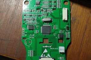
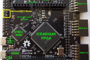
The MiCE47 is a small Cortex-M7 + iCE40 development board with an i.MXRT1021 µC and an iCE40HX8K FPGA.
The MiCE47 is a small Cortex-M7 + iCE40 development board with an i.MXRT1021 µC and an iCE40HX8K FPGA.
To make the experience fit your profile, pick a username and tell us what interests you.
We found and based on your interests.
MiCE47-v1.pdfSchematic Revision: 1 Licence: CERN-OHL-W V2.0Adobe Portable Document Format - 505.50 kB - 03/29/2020 at 19:57 |
|
|
MiCE47-v1.zipKiCad project containing schematic and pcb design files. Revision: 1 Licence: CERN-OHL-W V2.0Zip Archive - 1016.34 kB - 03/29/2020 at 19:55 |
|
|
... I finally managed to publish the design files of this project. Sorry for the enormous delay!
Why did all this took so long? – I originally had the plan to build the board, verify most of the functionality and then hit publish. Going down the rabbit whole of FPGA design, it took me much longer to get the correctly SRAM running (first it didn't work at all, later it didn't pass a random read/write test). Silly me messed up with the pin definition in Migen (it is very beneficial to assign all address lines to an IO pin!!!), which caused some serious lack of motivation. Now, before trying to publish the next/my current project, I want to make some progress here.
What is (not) published?
What is (not) coming aka the future roadmap?
This board was intended to learn some FPGA basics, BGA soldering and enhance my layout skills. So far I accomplished all three. I'd like to play a bit more with the i.MXRT1021 running tinyusb as well as nMigen on the iCE40, so new "softwork" can be expected for this board.
The hardware will not get any further revision. Most things are running and we have more powerful alternatives like the Pergola.
Special thanks to all people working on the open FPGA toolchain and Migen/nMigen!
Also thanks to Greg Davill for writing down his journey designing the Boson Frame Grabber and his beautiful electronics pictures! Your project motivated me to try soldering BGAs by hand :)
Sources of inspiration:
Currently I'm working on the firmware of the µC, especially the USB stuff. I already had a working demo that runs bare metal on the chip and let's you program the FPGA. It worked fine, but the architecture was a bit messy so I decided to rewrite it and incorporate FreeRTOS. While using the MCUXpresso IDE, I realized that it provides some quite interesting runtime analysis features. Equipped with my new debug adapter (I bought a J-Link EDU after having some hickups with my NXP Link2) I was ready to go...deep into the rabbit whole.
On the MiCE47 pcb I put down a single row pin header that is inspired by the STM Nucleo boards. Along with power and ground it provides an SWD interface including SWO and an UART port - so far so good. I found a nice introduction from NXP on how to use SWO with MCUXpresso and some of their µCs. The user guide says I have to configure the pin mux in order to use the optional SWO output pin. This made absolutely sense to me, as I assumed it is shared with JTAG's TDO pin which would be unused in normal SWD operation. The reference manual of the i.MXRT1021 series does say the chip supports SWD (chapter 7.2), but does not list the SWD interface in the pin mux table (chapter 9.1.1) explicitly. If you look at the reference board for the i.MXRT1021, the SWD interface is connected to the OpenSDA (p.13) as one would expect: SWDIO → TMS and SWCLK → TCK. SWO is not supported by the OpenSDA so it is not used. I interpolated this information and concluded that SWO would be multiplexed with TDO (some/many other µCs do). This is unfortunately not the case! On the current i.MXRT series the SWO output is not the TDO pin. Do search the datasheet explicitly or look in the pin configuration tool within MCUXpresso! The newer reference boards (also the i.MXRT1015) support SWO directly and therefore provide a more useful schematic (just the i.MXRT1021 board does not). Luckily I had the necessary pin on my PMOD header so it is easily accessible.
According to the SWO user guide, the next step is configuring and enabling the trace clock which is used inside the core. The configuration can be done using the "ConfigTool" within MCUXpresso (→TRACE_CLK_ROOT) or by code. Enable the clock by calling:
CLOCK_EnableClock(kCLOCK_Trace);
Now connect your debugger correctly, initialize the debug mode, hit on a breakpoint after the clock and pin setup is done and click on the "SWO Trace Config". There you can change the clock speed either by entering or auto detecting (great, what could go wrong?), start your analysis mode of choice and resume your debug session. Congratulation, you have done everything you are expected to do, yet nothing will show up (at least not for me).
While searching for a solution, I found this awesome article which describes how to use SWO on an i.MXRT1064 board. I followed the guide beginning to end and was eager to finally get the damn thing working. Well, it didn't. I suspected some issue with MCUXpresso and the J-Link (the article uses the LPC-Link2) or bad karma because I don't use Windows. It turns out that the solution is quite simple. When you use the auto detect feature for the target clock frequency, it seems to read out the actual core frequency of the µC aka 500 MHz. The linked article shows a screenshot with a 600 MHz clock for the i.MXRT1064 so I assumed this would be right. It is not, at least for my setup with the J-Link! You have to enter the actual frequency for the "CM 7 Trace clock" (TRACE_CLK_ROOT) that you have configured earlier! In my case it is up to 132 MHz for the i.MXRT1021. That's all.
The article also says you should enable a TPIU clock by
*((uint32_t *)(0x400E0600)) = (1 << 11); /* enable TPIU clock */
I don't know what this really is about. According the the reference manual (at least on the i.MXRT1021) this memory address is reserved and I could not find any information in the Cortex-M7 header files nor the ARM documentation...
Read more »Most versions of the i.MXRT microcontroller family do not include any flash for your program code. While this automatically forces you to buy an additional memory chip, at least you can choose what suits you best (QSPI-/Hyper-flash, µSD, etc).
When the µC is powering up, an internal bootloader is started to load the program code from the external memory device. It needs to know what kind of device it is going to talk to (basic initial configuration) and where it is connected.
NXP provides two ways of setting this initial configuration options:
Of course, there are also different boot modes to choose from (the bootloader needs know whether to read GPIOs) and this is done by pulling two GPIO pin states up/down:
This might sound a bit unusual, but the LPC4300 series (and probably other flashless ones) are quite similar to this. I planed to use the GPIO override mode, because my preferred QSPI-flash should work with default eFUSE settings and I wanted to keep flexibility. What could go possibly go wrong? - A lot! The FPGA is directly connected to the µC and should also be configured by the µC. When the board powers up, both chips will be initially unconfigured and only after the µC is up, the FPGA will come to life (if there is any bitstream). All µC I worked with before configure their GPIOs as inputs without any pull-up/down by default. Not so the iCE40! It sets the GPIOs to inputs with a pullup! Of course, I connected some GPIO override pins of the µC to the FPGA with its great pullup-by-default magic and created some fantastic boot configurations.
After realizing this issue, I wanted to boot directly from the default eFUSE settings because this should solve all problems right? As the defaults are exactly what I need for my flash anyway I don't even need to deal with the FUSEs and risk bricking my chip. Loading a program into RAM and executing it from there worked just fine. Loading a program into the flash seemed to work as well, but running it didn't work. My debugger always showed me a HardFault and stopped the execution at an unexpected memory address (for a simple "Hello world" example). It turned out, that this address belongs to the internal ROM where the bootloader stuff is stored. I was confused and disappointed.
In several locations in the reference manual and on page 72 in the datasheet you find the hint: "Boot Options, Pin value overrides fuse settings for BT_FUSE_SEL = ‘0’.". Nice, but totally unimportant for my setup so I did not care. If you read chapter 8.3.3 (page 189/190) in the reference manual about the "Boot From Fuses mode" you find another hint: "If BT_FUSE_SEL = 0, indicating that the boot device was not programmed yet, the boot flow jumps directly to the Serial Downloader.". This is very important and the exact reason why I spend nearly one week troubleshooting my board and software setup! If I chose the GPIO override mode, my FPGA created a wired boot configuration and all went wrong. If I chose the eFUSE mode, the µC decided to jump straight into the serial downloader because the fuse was not blown! There is an appnote about using the serial bootloader and NXP's computer software where they explain why this behaviour is great. Of course, I did not read this appnote and had no clue. Burning this one little fuse makes you loose the GPIO override forever, but it can save your day!
To configure the fuse settings I started the "MfgTool2.exe" to boot the chip into some special mode and then the "blhost.exe" tool for changing and verifying the eFUSE setting. Both tools and a documentation about the available commands...
Read more »
Create an account to leave a comment. Already have an account? Log In.
Become a member to follow this project and never miss any updates
By using our website and services, you expressly agree to the placement of our performance, functionality, and advertising cookies. Learn More

 jaromir.sukuba
 darkspr1te

 Eric Lind