I'm building a CMOS computer out of 70s technology to learn about the path we took to get from then to now, but also to develop a deep understanding of how each part of the computer works. I could read about it and it would feel like I understood the material while I was reading, but I would quickly forget. True understanding of a technology is demonstrated in the ability to use that knowledge to effect a change in the world.
I like to think of my hobbies and my work in the frame of working through a personal tech tree.

On this project, I'm applying that concept narrowly. I want to use a 74hc181 4-bit arithmetic logic unit and function generator as the ALU in my computer. I've build arithmetic units before, but not ones that also had a logic component. While looking at options for the ALU in this computer, I discovered the 74181 and it introduced me to a host of new ideas.
I knew that I could chain multiple counters or logic units together to go from 4 bits to 8 and so on and that this was done at the expense of an increasing propagation delay. The outputs of the first IC have to have stabilized for the outputs of the second IC to begin to stabilize and so forth. The more chips in the chain, the longer it takes for the final set of outputs to be stable. Clock the result too early and you get garbage bits.
The 74181 solves the propagation delay problem by using a method called carry lookahead to calculate whether an operation is likely to generate a carry. If you can do this, then you can do all your arithmetic operations simultaneously and greatly reduce the delay. I spent a bunch of time two days ago working out the boolean algebra and truth tables for P and G generations, once I heard about the idea.
The 74181 also has a clever internal implementation where it's 16 logic functions are added to the A input to create 16 arithmetic functions. This took me a while to wrap my head around. A bunch of it seems super obvious in hindsight, but the schematic and the design stumped me for quite a while.

The four S inputs select a function to apply to A and B...f(A, B). This boggled my mind when it clicked: the S inputs represent the answers to a 2-bit, 4-row truth table. S0 and S1 are inverted. So, when you set S == ( 1, 1, 0, 0 ) you are asserting "there is some boolean operation where for any A (1, 0) and any B (1, 0) the answer is 0, apply that function to my A and B". For any S you provide, you'll get back an answer that conforms to the truth table you've provided. If you set S == ( 1, 1, 0, 1 ) then you've given it the truth table for AND and it'll perform an AND on the inputs (remember the first two S are inverted). This just seems like a completely backwards way of thinking about the implementation of boolean logic and it's awesome.
Describing a function in terms of the set of its outputs, given a known and constrained range of inputs. My modern programmer brain wants to think of the options I could pick from like an enumerated menu or like some kind of library of operations. I thought of a function as a process, not as a mapping of input to output. I had lost sight of what a function IS.
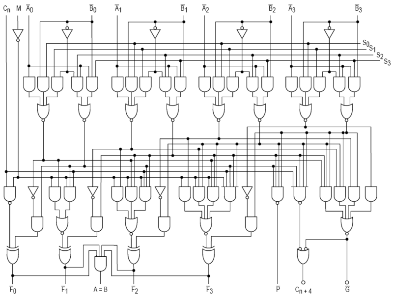
The first half of the circuit above implements the carry lookahead logic and the second half implements the truth table. The Cn signal is your carry-in so you can chain ICs. The M signal selects between logic or arithmetic modes.
LET'S BUILD A 74181
I think I understand this chip pretty well, but I'd like to build an interactive model of one. Working things out on paper and pondering the ideas in the logical schematic has helped a lot, but I think wiring up each of the gates by hand will crystallize things further.
Once I have my model built, I can sub in a real 74hc181 in the new computer. The IC will be much faster, but I can feel like I've mastered the large chunk of functionality that the chip aggregates.
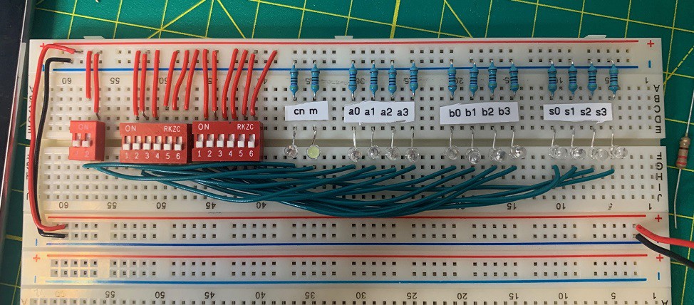
Tonight, I started on this sub-project by building an input terminal for the 74181 model.

A set of 14 DIP swtiches provide the Cn, M, A:4, B:4, and S:4 input signals. These can then be wired into the spiffy new 74hc gates I received today from Digikey and I'll hopefully end up with a working interactive 74181 ALU model.
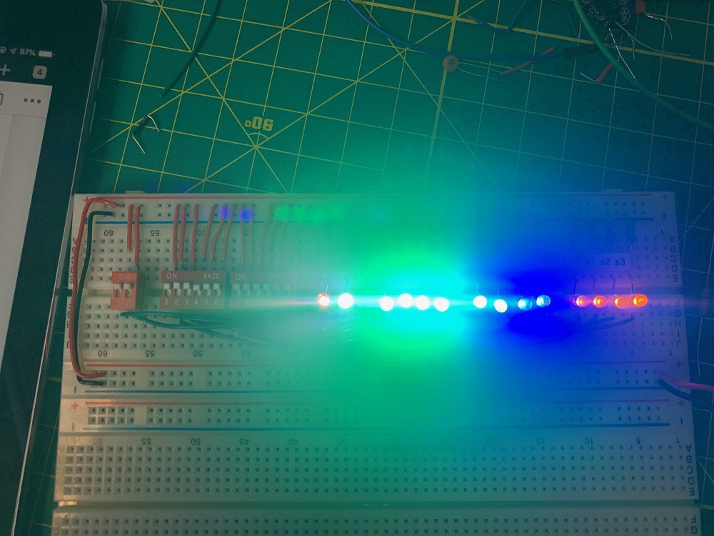
Oh and I increased the size of the resistors on the LEDs and some of the colors are just still too damn bright, so I'll probably do some experiments on which colors need what kind of reduction. I'm sure this is documented online somewhere, but I'd rather work through it myself.
GREEN LEDS OF BURNING DEATH

 Brandon Reinhart
Discussions
Become a Hackaday.io Member
Create an account to leave a comment. Already have an account? Log In.
the 181 is a massive beast! it looks simple on the schematic, but it's like molasses, sugar water boiled down to the essentials and..... totally SWEEEEEET!
Are you sure? yes | no
Though strictly speaking it's the ALU design, not the CMOS, that's from the 70s. In that era the 181 was implemented in TTL. It was only later that the HCT family, with TTL compliant voltage levels, was released to provide old logic IC designs in CMOS with all its attendant advantages.
Are you sure? yes | no
Yeah! I'm using CMOS in order to try and get a bit more speed and noise resistance out of this computer, over the TTL computer I've already built. Everything becomes anachronistic with this kind of project.
Are you sure? yes | no