Been a while since an update. Vacation took me away from the home for a bit, but I have been working on finishing a few modules.
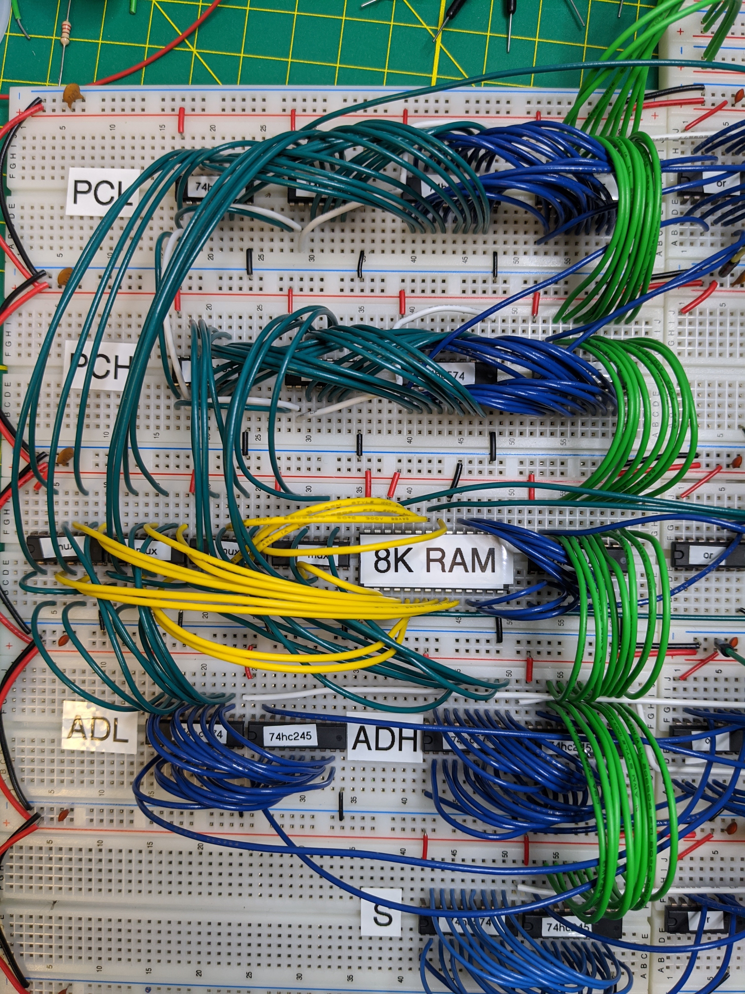
For RAM, I decided to create a control line that would select between RAM being setup by the address register or the program counter. This provides for addressing modes that want to lookup a 16 bit address at PC+1 and PC+2. I could have used some kind of internal register for this, but the RAM mux seemed like a more direct approach and I think covers all of my instruction architecture needs.
I accidentally ordered 512kx8 OTP EPROMs instead of the RAM chips I wanted, so right now I'm only running an 8k RAM. I have enough address lines for a 64k RAM, which should arrive this week. I couldn't actually find a 64k RAM chip on digikey, so I ordered 128k RAMS. Maybe I can add a bank line later.
The RAM tests out and reads and writes, address lines work correctly:

I ended up placing the PC above the RAM and the AD below. The 8K RAM label is on top of the RAM chip and to the left of it are 4 quad mux chips which select between PC and AD.
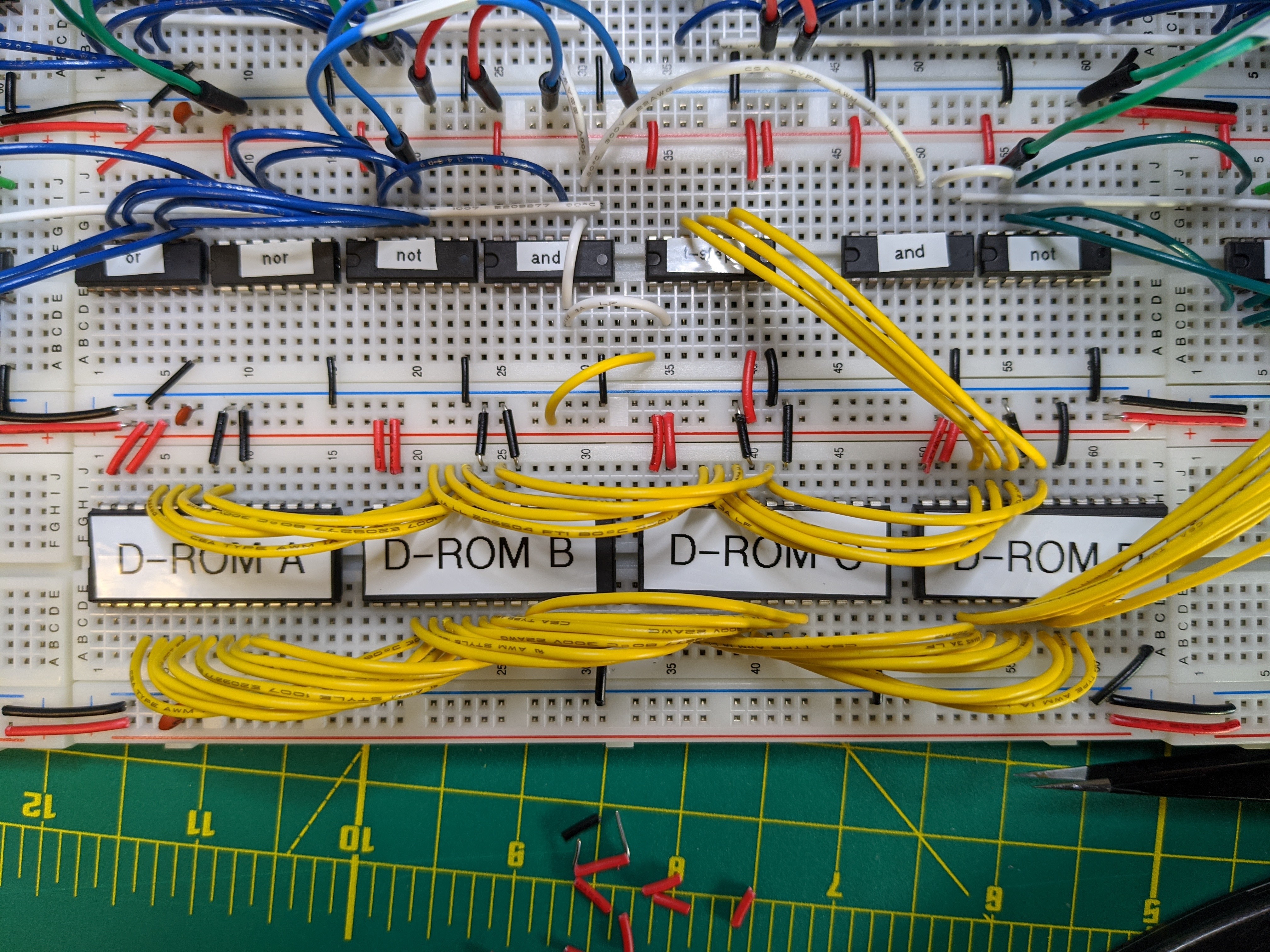
Once that was done I added the instruction register (IR) and a line of EEPROMs that will form the instruction decode logic. Instructions will be decoded by combinatorial lookup instead of microcode. Each EEPROM has 8 output lines giving me 32 control lines (for now).
I created a homemade EEPROM burner which I'll use to program each EEPROM.
Instruction bits are [ 8 bits ] [ 4 bits ] where the 8 bits are the OP code and the 4 bits are time step, so these uniquely address 256 opcodes with 16 time steps. I won't need 16 time steps, so it's possible I could use a bit on something else.

In the image above, the EEPROMs are setup to always output and never write. There's a little 4 bit counter that drives the time step.
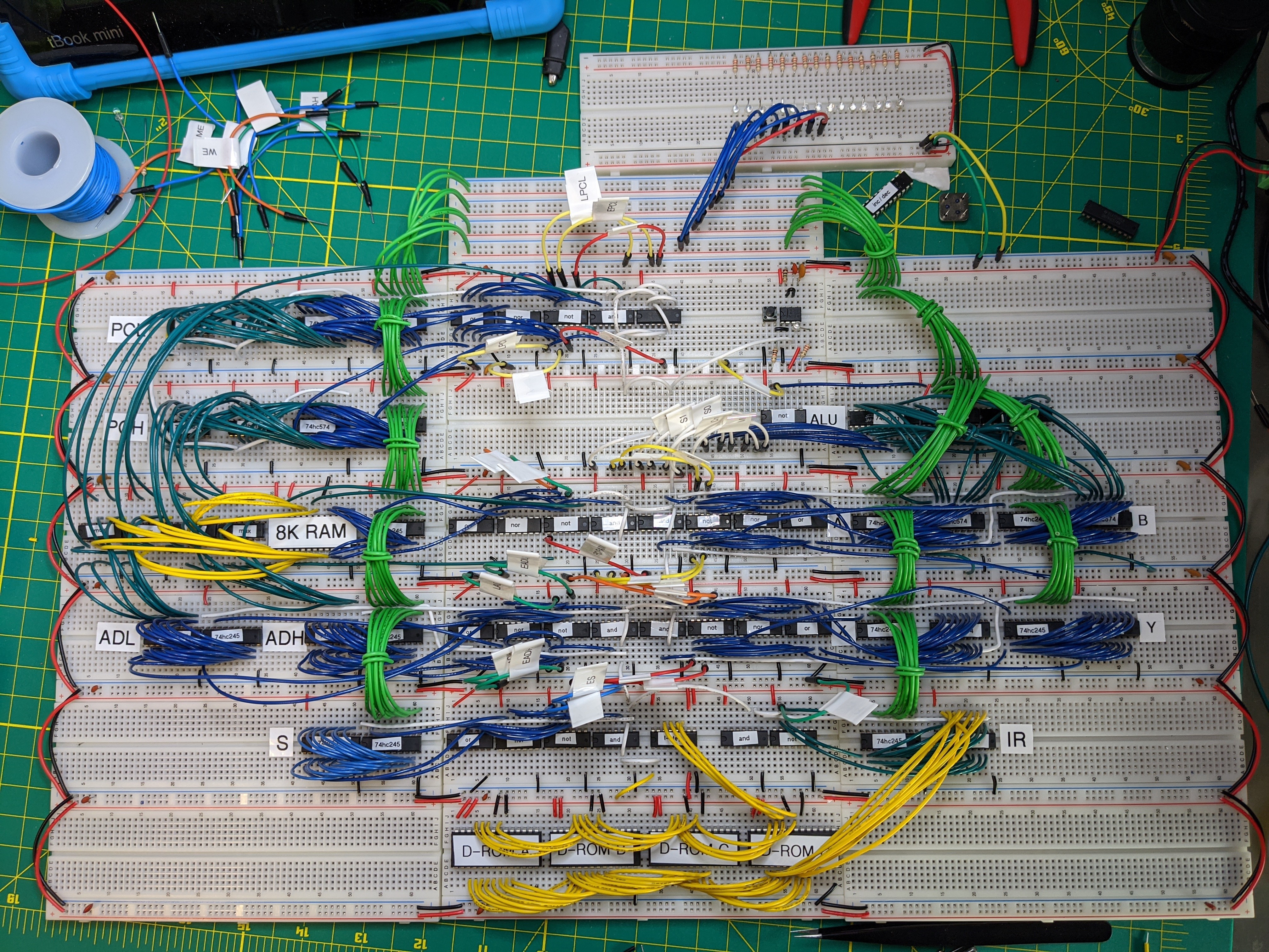
And here is the overall computer so far:

The tasks remaining:
- Add a variable speed 555 timer clock circuit for low frequency operation (for debugging).
- Replace the 8k RAM with a 32k RAM.
- Write the arduino code that will output the decoder tables and burn the EEPROMs.
- Author the instruction set. This is what will generate the decoder tables.
- Wire up the control lines (replacing all those flagged lines in the middle with lines from the EEPROMs).
- Create a boot loader circuit driven by another EEPROM. This circuit would transfer test code or the kernel into the RAM when the computer is turned on.
Then write some programs to test the range of functionality.
I'll need to add a flag status register, but I figured I'd wait until I was creating those instructions. Flags should be able to bolt onto the existing design without much hassle.
If I get through that, I'll move onto the video card. Long term project path is to create a video card and an interrupt based keyboard interface.
 Brandon Reinhart
Discussions
Become a Hackaday.io Member
Create an account to leave a comment. Already have an account? Log In.
An alternative to boot loading from an EEPROM is to boot load from an arduino that transfers the code/kernel to the RAM. Maybe if I get a kernel I like, later, I can use those OTP ROMs and just have a kernel ROM bank!
Are you sure? yes | no