Typical Application
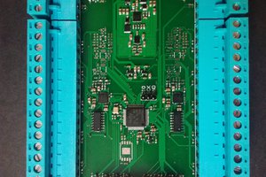
> AS-6408 have two output ways, one is 64CH <-> 8CH and one is 64 <-> 1CH, the 1CH output is after the 8CH output and they can working at the same time.
> AS-6408 have onboard UNO CORE design , that means it can be working alone to process the 64CH input and read by A0 to A7 with 10bit ADC , and then sent data via TXD/RXD , if you using the RF UNO CORE it can be implement wireless data acquisition very easy.
> The input signal level should not exceed VCC (Range of 0 to VCC), otherwise it may cause signal distortion.
> The control signal is standard COMS TTL-3.3V level.
> Main IC using 74HC4051D from NXP , the datasheet link : https://www.nxp.com/products/automotive-products/discrete-and-logic/logic/analog-switches/8-channel-analog-multiplexer-demultiplexer:74HC4051D-Q100?fsrch=1&sr=3&pageNum=1
Specifications
Power supply
With UNO CORE : 3 to 15V Without UNO CORE : 3 to 20V ON Resistance : 125ohm Change in ON Resistance : 50ohm OFF channel leakage current : + -0.01nA Capacitance Input : 30pF INPUT Low : Max 1.5V INPUT HIGH : Min 2.2V
Operation Temperature : 0°C to 55°C Operating Humidity : 0 to 90% non-condensing Storage Temperature : -20°C to 65°C
Propagation Delay Time Signal Input to Output : 10nS Address-to-Signal OUT : 120nS Cutoff (-3dB) Frequency : 20MHz THD(Total Harmonic Distortion) : 0.12% Address-or-Inhibit-to-Signal Crosstalk : 65 mV PEAK
Purchase link:https://www.ebay.com/itm/222827261696

 guilldeas
 Manuel Tosone
 Bud Bennett
 NotBlackMagic