 agp.cooper
First Steps
There is a lot of work setting up the interface between the schematic capture and PCB layout applications and the auto-routing applications. So I will just read in a simple text files to begin.
The Schematic
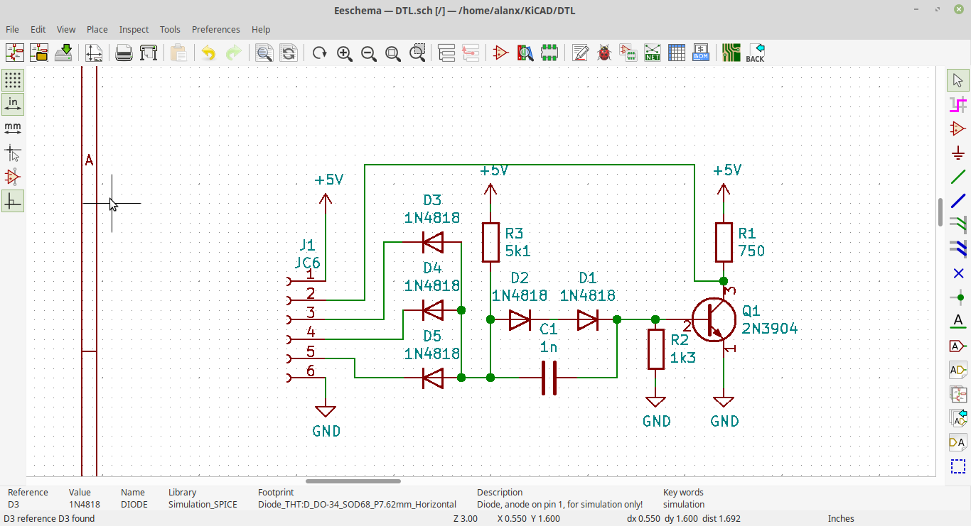
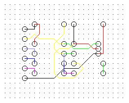
One of my first PCB schematics was a DTL (Diode Transistor Logic) three input NAND gate. Here is a KiCAD version.
First the KiCAD schematic:
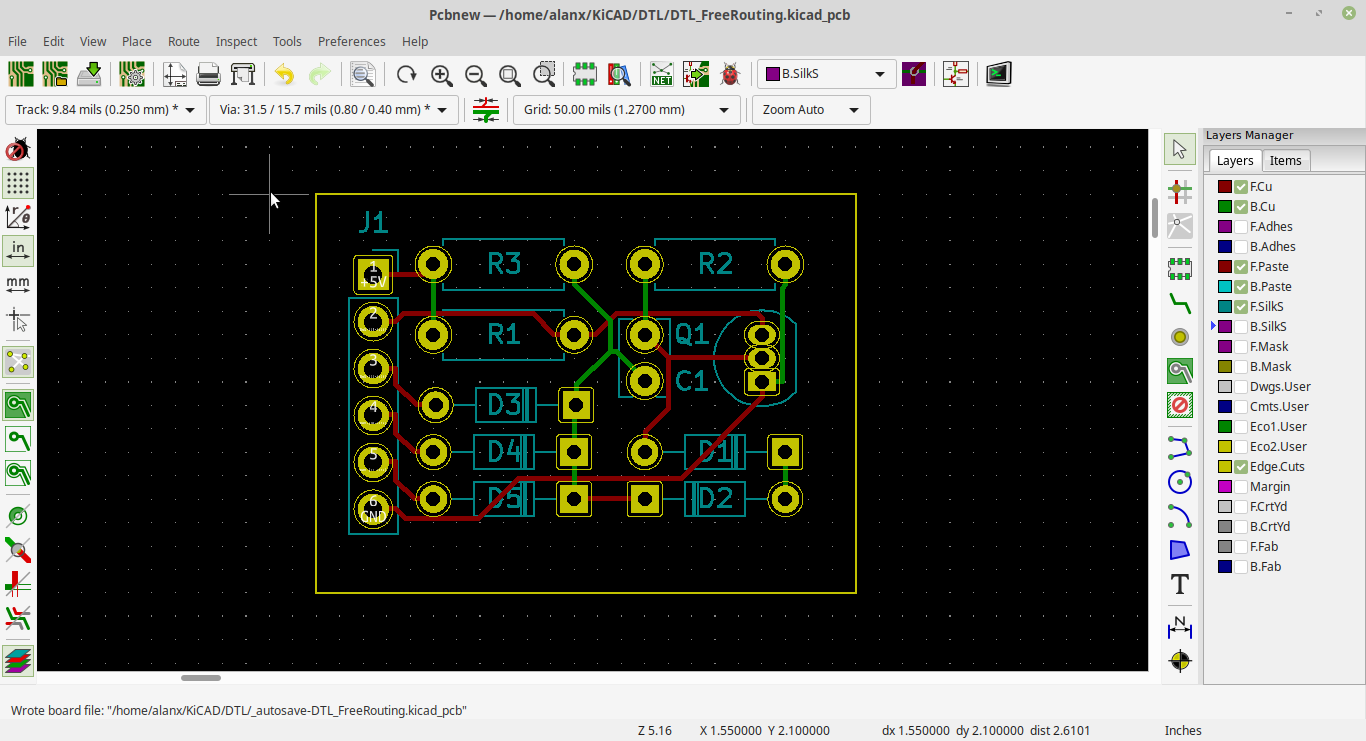
And the KiCAD PCB:
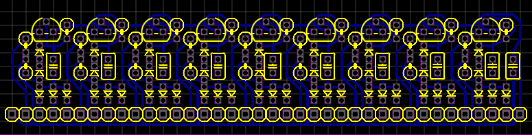
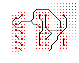
Now I have tried to get a single sided PCB version of this design (in Eagle and EasyEDA) but it is surprisingly difficult to do. KiCAD does not even offer the option. In the end I had to hand route a design (okay it has nine copies):
With a bit of imagination you should see the KiCAD PCB here (map.txt):
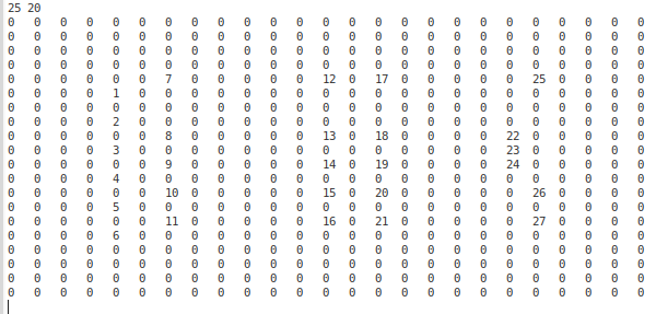
And the links list:
SRC DST
 1    7
 7    8
 2   13
13   22
 3    9
 4   10
 5   11
 6   24
24   25
12   14
14   19
14   15
15   16
16   21
17   18
18   23
18   20
26   27
After a Day of Coding
Here is a series of images as I debugged and got the penalty function working.
Well its just about getting something on screen to look at!
I want to penalise paths that get too close to the pins (thus the small red dots):
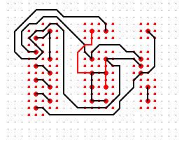
Note: The red tracks failed to find a legal path. A diagonal path between tracks was consider illegal.
Here is a working case:
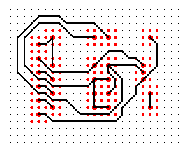
Note: The links are exactly honoured and thus the ugly links.
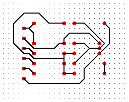
Finally with a pseudo-Steiner Tree modification gives a pretty reasonable result:
So for a single side PCB I have a result that works (for the small example).
So how is that, all of the above in less than 600 lines of code!
A lot more to do, add multi-able layers and back-tracking when the algorithm fails.
Update
Added some code to randomly swap around the links to see if I can improve the result.
I gave the router 1 second, it looked as 2083 options and reduced the penalty from 682 to 582:
I have been looking at the passes that failed to determine if there is an easy heuristic I could apply. Even in the above image the I can see faults that could be fixed that would improve the success rate.
A couple of papers suggested:
- Sorting the nest by complexity (i.e. number of bounding square interactions) or at least net length.
- And if that fails, then route the conflicted net on the next layer.
Currently I completely randomise the links for a run and run a many as I can in one second.
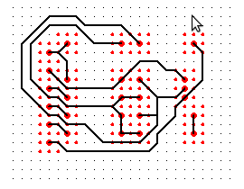
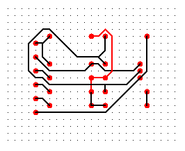
Here is an example where I use the above approach (i.e. a single run) but include a congestion penalty:
 You can see that the congestion penalty has moved the tracks away from the pins (and other tracks) leaving space for later tracks. This in my mind is a pretty good result (for a single run). Without the congestion penalty you get:
Code
I have posted the code for the above.
Paper by Eric Rosenberg on Iterative Routers
I found a paper by Eric Rosenberg that describes an iterative method for improving the router performance. Here is a simplified version of his algorithm:
- There is no prioritisation of the nets (or links).
- Initially with the supply/demand router, all nets are routed without regard to conflicts and can share the grid node (or cell). After each iteration, the conflicted cells are given a penalty with the "hope" that it will resolve the conflict.
- With each iteration the penalties of the remaining conflicted cell are increased.
- Eric Rosenberg proposes that if a solution cannot be found after a number of iterations, then the conflicting nets are ripped up and rerouted.
It should be noted the algorithm can be unstable and much of Eric Rosenberg's paper is about approaches to resolve this issue.
AlanX
Discussions
Become a Hackaday.io Member
Create an account to leave a comment. Already have an account? Log In.