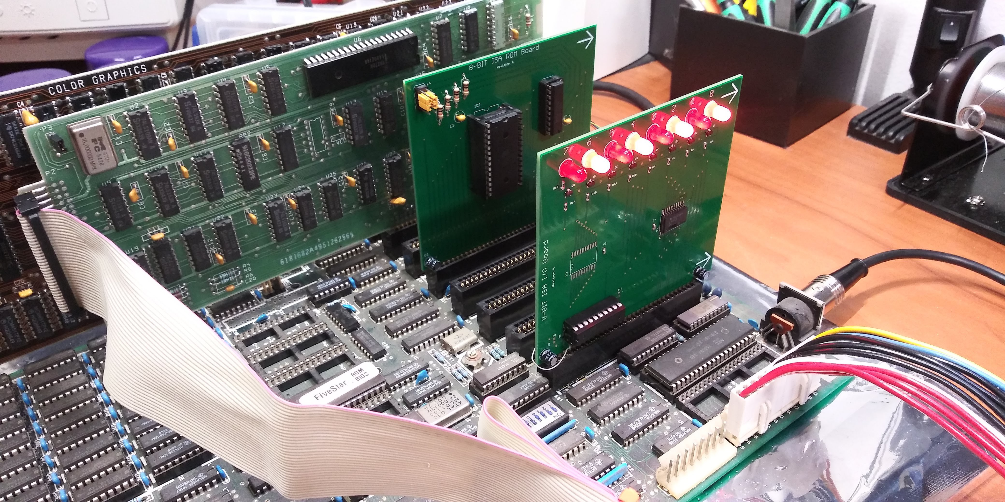
I assembled the 8-Bit ISA I/O card earlier this week, but realized that it had some "issues". My design uses two 74LS374 edge trigger latches for both the read and write. However, all of the example design use a 74LS373 level triggered latch for the read, and a 74LS244 or 74LS245 for the read. Fortunately the 374 and 373 both have the same pinout and pcb footprint, so i was able to just substitute a 373 for the 374, and BINGO, it worked! Pictured is the the 8-Bit ISA ROM Board executing code to write the value of 0x55 to the port 0x300 on I/O card. Port 0x300 to 0x31F were originally defined by IBM for "Prototype Cards". I really have to hand it to IBM, they really had a way of thinking their designs through and leaving room for development...
 Dave's Dev Lab
Discussions
Become a Hackaday.io Member
Create an account to leave a comment. Already have an account? Log In.