Bernhard "HotKey" Slawik
-
CP/M on VGL: Issues and Solutions (Updated!)
11/04/2019 at 10:46 • 1 commentMost of the inner workings of the V-Tech Genius Leader / PreComputer have been discovered. Even some lesser known functionality, which is hidden inside a proprietary silicon, is understood. Especially, how the LCD, the keyboard matrix, printer port and most of bank switching works.
Now for the philosophical question: What should we do with it?
When talking to people, most of them agree that getting an own operating system to work is priority 1. But on which OS to focus on is not fully clear. Personally, I would prefer CP/M, since it is the Z80 operating system with the most impact and support.
There are two problems with CP/M on this "toy hardware":
- CP/M requires a disk drive. The V-Tech computers don't have one. But since we do have a cartridge port and proof-of-concept memory-mapped I/O, as well as a working serial port, getting some sort of SD card reader or serial storage medium to work should not be a big problem. In the meantime we can use bank-switched ROM/PROMS/SRAM or load software from the serial port (already working!)
- CP/M requires RAM to start at memory address 0x0000, since this is how CP/M programs interface with the BIOS/BDOS drivers. See: http://www.primrosebank.net/computers/cpm/cpm_structure.htm
The latter problem is a bit more tricky. See, on power-up the Z80 CPU jumps to address 0x0000 and starts executing the instructions located there. That's why there is a big system ROM located at that address.
Bank switching the system ROM
After thinking long and hard, I decided to leave the "non-invasive" route and add a little hardware modification to my beloved Genius Leader 4000 Quadro. I opened it up and put wires to the "Chip Select" lines of the ROM, the RAM and the cartridge port. Fortunately, these 3 lines are conveniently located on one corner of the PCB (near the cartridge port) and each go through a wire bridge. It is really simple to cut these bridges and add some wires, so they can be connected/disconnected at will:

"Chip Select break out" connector (upper right) allows disconnecting the internal ROM at will. A simple "Bus Doubler" (bottom) allows inserting two cartridges at once. You'll see why. On its own, this is not a very helpful mod :)
But now you can insert a ROM cartridge and use a different "Chip Select" pin (the new "internal ROM ~CS" instead of the default "cartridge ~CS" on Pin 35). A slight modification in your code (segment now needs to be 0x0000 instead of 0x8000) and your external ROM cartridge can now act as the internal system ROM! That means: Now we have a full 32kB of additional address space without de-soldering the internal ROM!
But be aware that the internal system ROM also contains crucial hardware initialization functions which now need to be done in our own ROM. This includes the LCD initialization sequence, resetting all the MUXes and bank switchers and -most importantly- reacting to interrupts and polling the keyboard matrix.
My current implementation works fine in the MAME gl4000 emulator, but still has some issues with the LCD (one line is not showing - using a non-standard DDRAM mapping) and the keyboard is not working reliably. This still needs some more research to get right. But enough to continue with some more experiments...
Booting from RAM
But now for the really tricky part: As I said, CP/M needs RAM to be at 0x0000. But since RAM is -usually- volatile, we can not simply solder in a SRAM IC and call it a day. It won't boot, since it is empty.
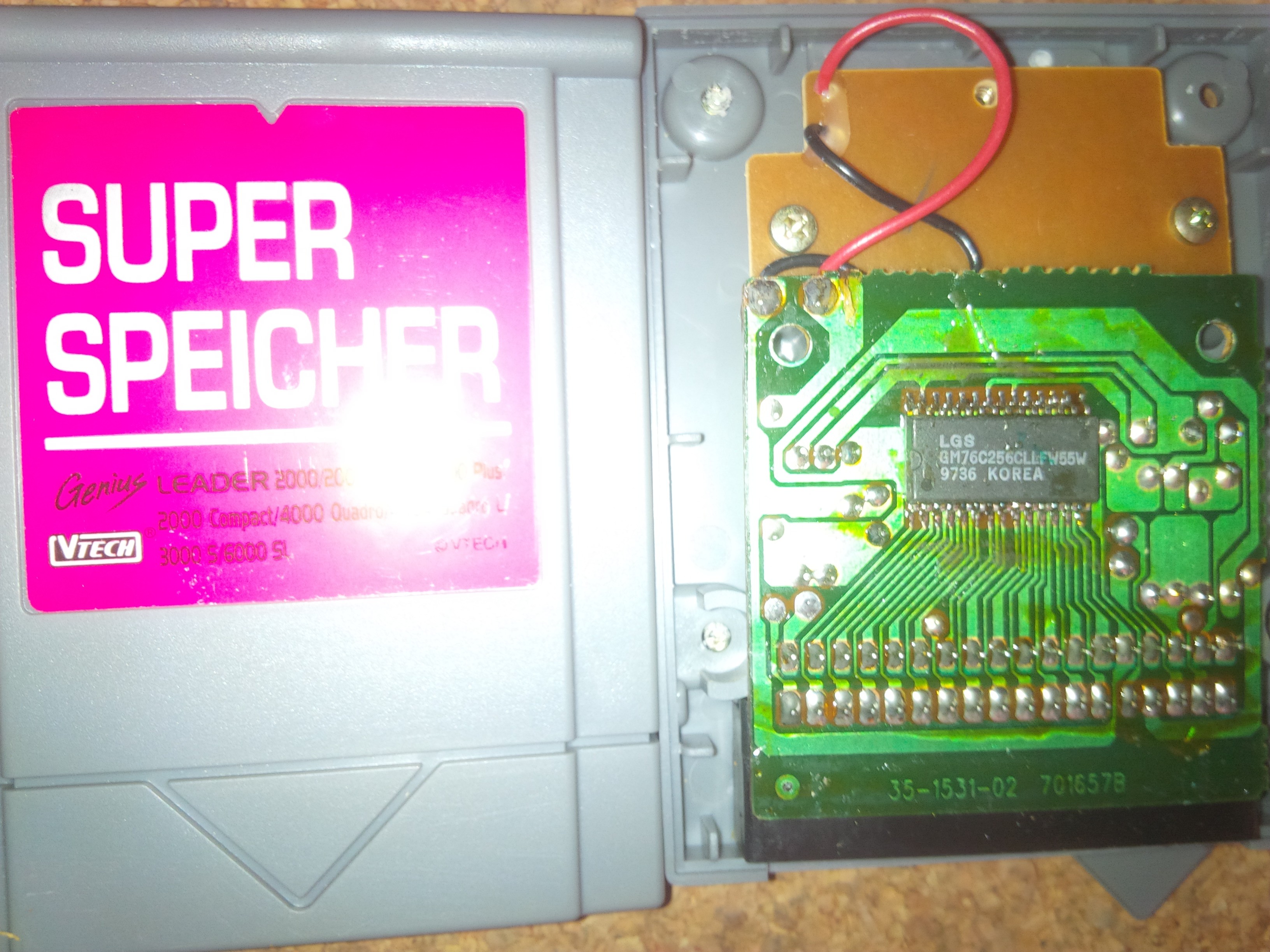
My current idea is to use the battery backed SRAM cartridge VTech Super Speicher 32KB for that. It contains a 32 kilobyte SRAM IC, as well as a coin cell battery and a few transistors (to invert signals and switch from internal to external power).
![]()
![]()
It should be possible to boot from a custom system ROM (mapped to 0x0000) while having the SRAM connected to the cartridge slot (mapped to 0x8000). Then, prepare/bootstrap the RAM contents to contain the initial jump instructions. When this is done, ROM and SRAM would "swap places" (remember, the "Super Speicher" is battery backed and won't lose its contents) and the system should now be forced to "boot from RAM".
At least that's the theory.

Bus Doubler in action: ROM at 0x0000, RAM at 0x8000 I tried it yesterday in the late, late evening. And while the initial bootstrapping of the SRAM worked, the system did not boot from SRAM once I swapped it in as "system ROM". The screen just went weird (reset loop?) It seems like there is still some interrupt or timing issue... But I won't give up just yet!
Also, creating the ROM image is not trivial, since it needs to contain code segments that are compiled for the 0x0000 segment, as well as code that is run, once it is mapped to the cartridge port at 0x8000. The current build tool chain now contains some calls to "dd" to extract and merge parts of different binary images. Stuff you shouldn't be doing on a Sunday night at 2am...
Do you have any better ideas to get CP/M running? (e.g. re-locating programs to use 0x8000 instead of 0x0000?) Let me know!
Update: It flippin' works!

Booting from RAM: YES IT CAN! I can't believe it: I just fiddled around with the initialization sequence a bit more and... HEUREKA! IT BOOTS FROM SRAM!
Of course, this is not a real CP/M system, yet. But I had to give it a name anyway, so I just went straight for it. "Aim high!", they say ;-)
So: This solves the main issue of getting CP/M up and running: Booting from address 0x0000. I am pretty sure, we will find an even more elegant solution of disabling the internal system ROM (using the "A17" and "A18" lines? Or using the software controlled CAPSLOCK LED for it?). But soldering 2 wires to well-accessible parts of the PCB is already quite easy to pull off.
And suddenly, there is the biggest question yet:
When will it play the original ZORK?
Soon, I hope! Will we master it in 2019? For the holidays? Let's find out together!
-
A Strong Community!
11/04/2019 at 09:58 • 1 commentWow! Since hackaday published an article about this project ( https://hackaday.com/2019/10/14/repurposing-a-toy-computer-from-the-1990s/ ), messages come pouring in from all over the world! And it fills me with joy, how many people like this project and have even already done amazing research in the same direction.
Worth mentioning is the work done by @Alex Rider about the french "YENO Compusavant". which seems similar to the "Genius Leader 6000 SL". Check out his website for more info: http://alexandre.botzung.fr/
I think I will be setting up a Github repository to merge all findings in an "(Unofficial) V-Tech 8-Bit DevKit".
So: Stay tuned and stay curious!
Bernhard
-
Retrofitting a printer port
10/28/2019 at 19:14 • 4 commentsSince many owners of models that don't have a printer port pointed out: There are some unpopulated parts on their main PCB and asked if the printer port could be retro-fitted.
Well, I guess so!
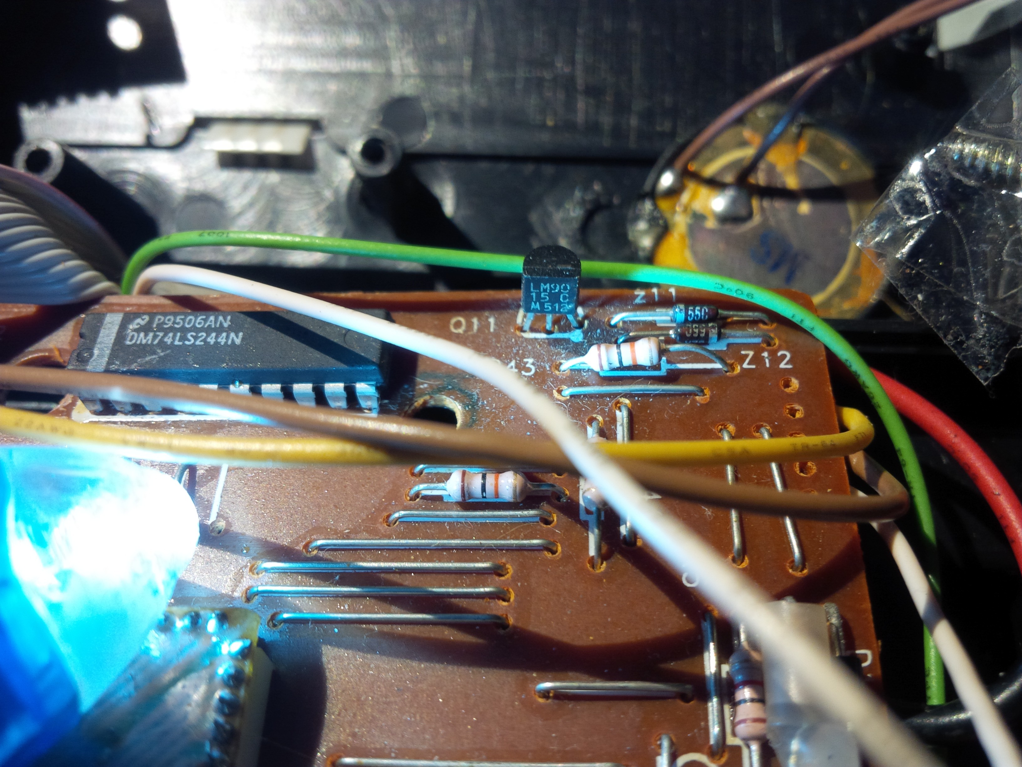
![]()
So there are only 8+1 bits in the OUT direction and a single bit in the IN direction. The latter is used to tell if a printer is connected and ready.
As I have found out, it is also used for PC communication: Using the 8 data output bits, the notebook selects, which bit of the incoming byte it wants to be set on Pin 11. So I guess the PC-Link cable contains an 8-bit "AND" IC.
But enough chatter: Here is the list of missing parts for the printer port:
Component ID Markings Description <IC> P9506AN / DM74LS244N 74LS244N Octal Buffer <Connector> Ribbon cable to D-SUB 25 Ribbon 1-9 to Pin 1-9
Ribbon 10 to Pin 11
Ribbon 11 to Pins 18...25 and Shield
(where Ribbon 1 is near C93)C12 403 40 nF capacitor C93 222 AEC 2.2 nF capacitor R35, R41, R42, R43, R44 brown black orange 10k resistors Q10 LM90 / 14C / M[otorola] 521 NPN transistor Q11 LM90 / 15 C / M[otorola] 512 PNP transistor Please let me know if you find any mistakes. Also, drop me a line if you managed to pull off the upgrade procedure. I'd love to hear about it!
Happy upgrading!
-
BusF###er Cartridge, Friends and DOS
08/03/2019 at 15:40 • 0 commentsI haven't written much about the PCB I have created to interface the V-Tech cartridge bus. That's mainly because I just haven't had enough experience designing PCBs so far, and didn't want to unleash a poorly designed and untested layout to the masses. So I spent 2018 doing a lot of design iterations on the so called V-Tech BusF###er cartridge, making it more configurable, reliable and debuggable.
It is 2019 now and I finally dared to send the first PCB layout to the manufacturing plant... And I was pleasantly surprised about the quality of the boards -- and disappointed about my skills ;-) as I simply made a lot of stupid mistakes (connected wrong GNDs, didn't leave space for additional caps or pull-downs, made important traces impossible to reach etc.)
But as of July 2019, there are now several Rev C boards on my desk, each successfully serving a custom boot ROM and having latches and registers to allow for memory mapped I/O to custom periphery! That is: 8 bits of data going onto the bus, and 8 bits going out. That is enough for letting 8 LEDs blink or querying the state of 8 push buttons. (If this would have been a commercial product back in the 90s, I would definitely have wanted one! Imagine "V-Techuino" ;-) ). Oh, and the boards are now daisy-chainable! The more boards you add, the more fun there is, of course.
On the software side I have developed a Serial Loader ROM, which allows code to be sent over a USB-to-serial FTDI cable connected to the V-Tech printer port. Just one click and your code gets compiled, transmitted, relocated, linked and run. Hardware and software development is now much, much quicker!
I have also been contacted by a chap named Erik Olsen and we might be cooperating on this project from here on. We both dream of having some sort of DOS running on the PreComputer and we have already made some serious progress. Maybe using FRAM or re-purposing GameBoy Flash Carts.... hmmm..
Stay tuned!
-
Z88DK and SDCC
08/03/2019 at 15:11 • 0 commentsThanx to the help of some great people at the Z88DK forum (hi alvin!) I was able to add some rudimentary support for the V-Tech Genius Leader / PreComputer to the Z88DK development suite. Just have a look at the platform called vgl to see some of my demo programs. It was quite a hassle for me to get used to implementing the necessary "newlib" I/O functions. Especially so, as they differ slightly for the 1000, 2000 and 4000 series.
Going forward, though, I recommend using just the simpler SDCC compiler if you want to get started on V-Tech development. You will not be able to benefit from the extensive demos of the Z88DK, but the overall installation and maintenance is much easier when just calling sdcc. The V-Tech headers and includes will be available on this project page or my github page soon.
-
2017 - Road to Genius
08/03/2019 at 14:39 • 0 commentsSo, another late night I searched eBay for "learning notebooks" and instantly got dozens of hits for notebooks by manufacturer V-Tech (well known for its Disney licensed/branded learning notebooks - there are thousands of them on eBay!). I narrowed down my search to the most "serious" and "boring" looking ones, not the colorful and whimsical ones. And that's when I got hooked on the vintage V-Tech Genius Leader series of learning notebooks (known in the US as V-Tech PreComputer or sometimes YENO MisterX)
Those things go for about 5 Euros on eBay, are available in vast quantities and seem to have big similarities among the different models - there seems to be some sort of proprietary V-Tech "platform" shared among those devices, and most of them even come with a parallel printer port and/or a mouse!
I wand to know more!
I bought all of them.
"Now this is going to be a real challenge", I thought. Proprietary devices which -I suspect- have only a single "magic" chip-on-die inside them and no official documentation available whatsoever. This could be very challenging, but also very interesting!
Spoilers: It was interesting :-D
For days the mail man brought one Genius Leader after the other: 2000, 4000, 4004 Quadro L, 5000, 5005 X, 6000 SL, 8000 CX, ... I started feeling like a hoarder. And so did my friends. But my brother simply called it Nerdophilia :-) Thanx for the understanding, bro!
I found out that most of the models share the exact same cartridge port design. You normally put new programs in there or add additional memory for the word processor and the built-in BASIC interpreter (yes, they can run BASIC! <3 <3 <3). So the cartridge port is the place I have to put my focus on: When cartridges can transfer data (and maybe program code) to the computer, why shouldn't I be able to do the same (or more)? It's pure logic.
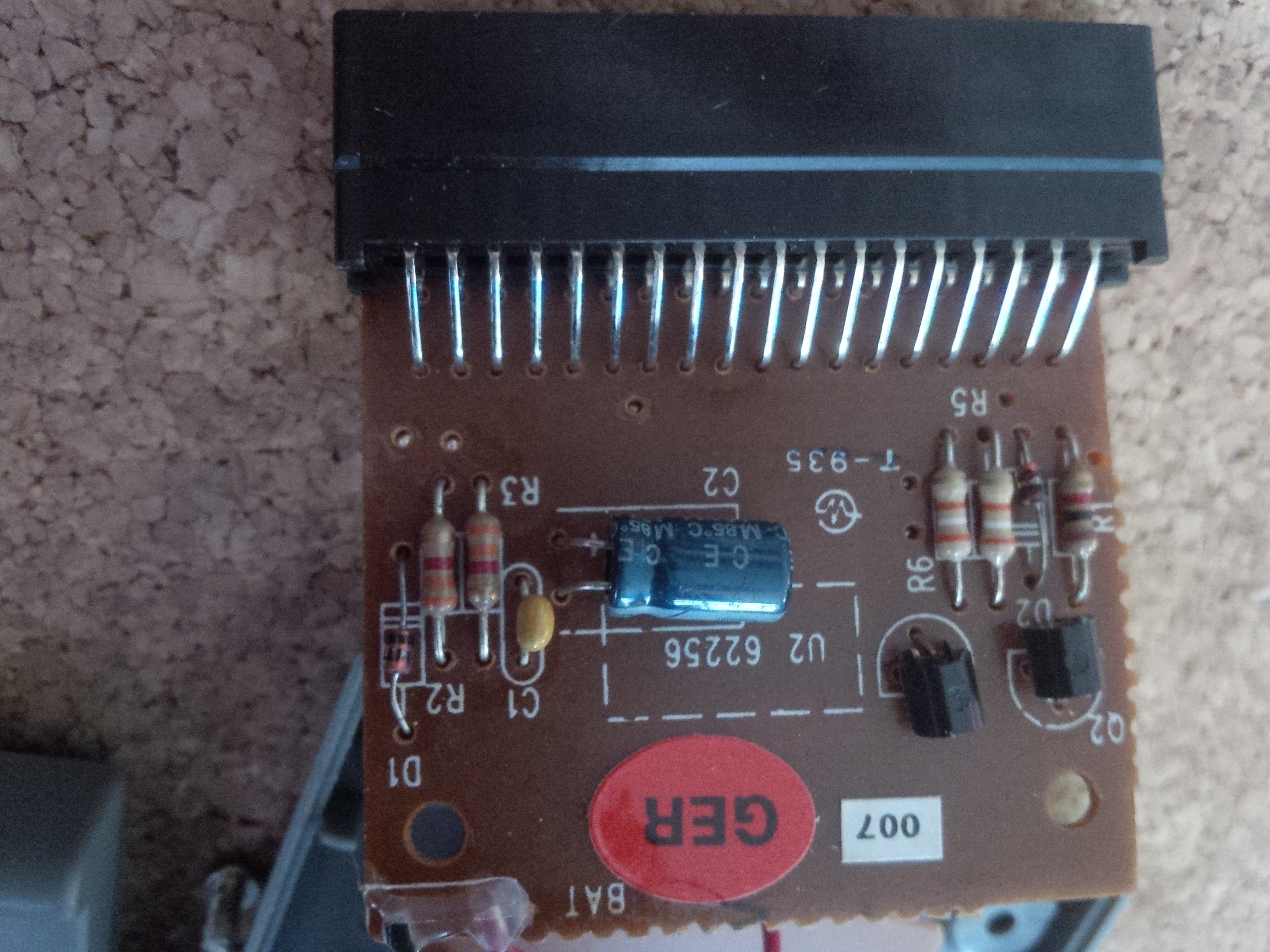
The most common physical form of cartridge port consists of an edge connector with 2 rows, 18 pins each, so 36 pins in total. The cartridges have the female connector on them, the main board exposes a card edge. Physically, the cartridge side almost resemble an old 5.25" floppy drive connector, except the floppy cable misses 2 pins (1 pin per row), so it is shorter. But that didn't stop me from trying it anyway ;-) I used a hot cutting knife and made the slot wider on one side. Fortunately, by opening up 3 cartridges, I saw that the first 2 pins (pin 1 and 36 by the V-Tech labeling) are not used! So I can just put in my own cable and do not need to care about pins 1 and 36. The plan was to hook up an Arduino and watch what kind of data flows through those 36 (or 34 if you want) wires. There is NO documentation available, so what should I do? Also, the cartridges I opened only contained one single V-Tech branded chip (some proprietary ROM chip?), so no information on what the pins could mean. Well, some of the outer pins are usually GND and +5V, but that's all that's obvious. I eBayed some more and finally bought a Super Speicher 32K -- a cartridge that does not contain a program, but is instead used to store data (BASIC programs or text files from the word processor). So there is no ROM chip inside this cartridge, but must either contain an EEPROM, FLASH or SRAM+battery to be able to hold information. And it was the latter: A coin cell battery and a 32 kilobyte SRAM chip. Lo and behold: Finally, a non-V-Tech branded chip! It's marked LGS GM76C256CLLFW55W and that means it is a Hynix 32K x 8Bit CMOS SRAM. Wonderful! By looking at the data sheet of that chip and how it was connected to the cartridge port, I could easily find out what each pin meant. Or at least 24 of them (GND, 15 address bits, and 8 data bits). That should do for a first test. I used my odd cable contraption, connected it to the notebook and the Arduino and dumped all bits to the Arduino serial monitor. I was prepared to see activity when I pressed the "CARTRIDGE" button, but in fact there was activity all the time. That means: I just tapped into the internal bus of the computer - the "spinal cord" of the notebook so to speak. It is now possible that I can see the computer thinking through that port - that is something that was completely unexpected and absolutely satisfactory for me. :-D Now I knew that it was not crazy to have so many of those notebooks - it all seemed to have purpose now! :-D First, I used an Arduino MEGA (I needed up to 36 input pins) to catch all the data, but quickly found out that it's too slow to catch a reasonable amount of data without missing too much of it. Although the Z80 processor is relatively slow in today's standards, it still ticks through its memory at a speed of up to several million steps a second. That is a lot of bits to print to a serial console...
Luckily, I still had an unused Arduino DUE somewhere, which has the same amount of pins and runs at a much higher speed (84 MHz vs 20 MHz). Also, the serial port can handle much higher baud rates (theoretically up to 480 MBit/s). That should suffice :-D
I could now clearly see certain memory regions lighting up according to different events (keyboard input, running BASIC, writing long texts, playing games) - that was truly mesmerizing! :-D
But even though I did get a glimpse of the address layout, the speed was still not fast enough to read from (not even talking about writing to) the Z80 bus quickly enough without using some completely different hardware: Either "new school" FPGAs or "old school" 74 logic.
It was clear to me that I had to dive deeper into hardware development and start creating my own expansion cartridge that could correctly handle the Z80 bus. That was what I did next.
-
Back in 2016...
08/03/2019 at 14:15 • 0 commentsOnce upon a late night in late 2016, I stumbled upon a "children's learning notebook" by a German board game company Ravensburger. For only a few Euros I gave in to my curiosity and just bought it. Maybe as a fancy Raspberry Pi notebook case using its original components (screen, keyboard)? I had a lot of ideas.
It arrived, I switched it on and was happily greeted by a friendly female voice (nice text to speech), inviting me to commence in a round of math quizzes. Cute! I played some rounds, tried out most of the integrated programs, when I suddenly stumbled upon something quite geeky: Productivity programs! There seems to be more to that device than just plain learning games!
The fact that it comes with an integrated word processor, which has a menu item called PC-Link intrigued me - Could I connect it to another computer? An Arduino? A Raspberry Pi? ESP8266? Well, I did not find any information about the "PC-Link" feature on the internet. I even contacted the company's support directly. And they scanned the original manual and sent it to me as a PDF! Thank you, Ravensburger support!
But no matter how hard I asked/searched, there seems to be no cable or software available these days. The computer uses a standard 6-pin Mini DIN jack to connect to a printer. I searched eBay and bought it. Then I shoved some wires into the DIN-port and connected an Arduino between the notebook and the printer. Then I started the word processor, wrote some words and selected "Print" from the menu and watched asthe bits flew between the computer and the printer... I quickly saw that it looked like some kind of SPI protocol. That was fun!
So this showed me that data transmission is physically possible, and there is some level of hackability to these devices. But what about running own code? I could not find any cartridges (yes, it has a cartridge port) so there is no way of finding ROM dumps to play with. So I first stopped there.
But wait! There are so many other "learning notebooks" out there! Off to eBay!!!
(to be continued)
V-Tech Genius Leader / PreComputer Hacking
Turning a toy into a hardware tinkering platform