 John Lonergan
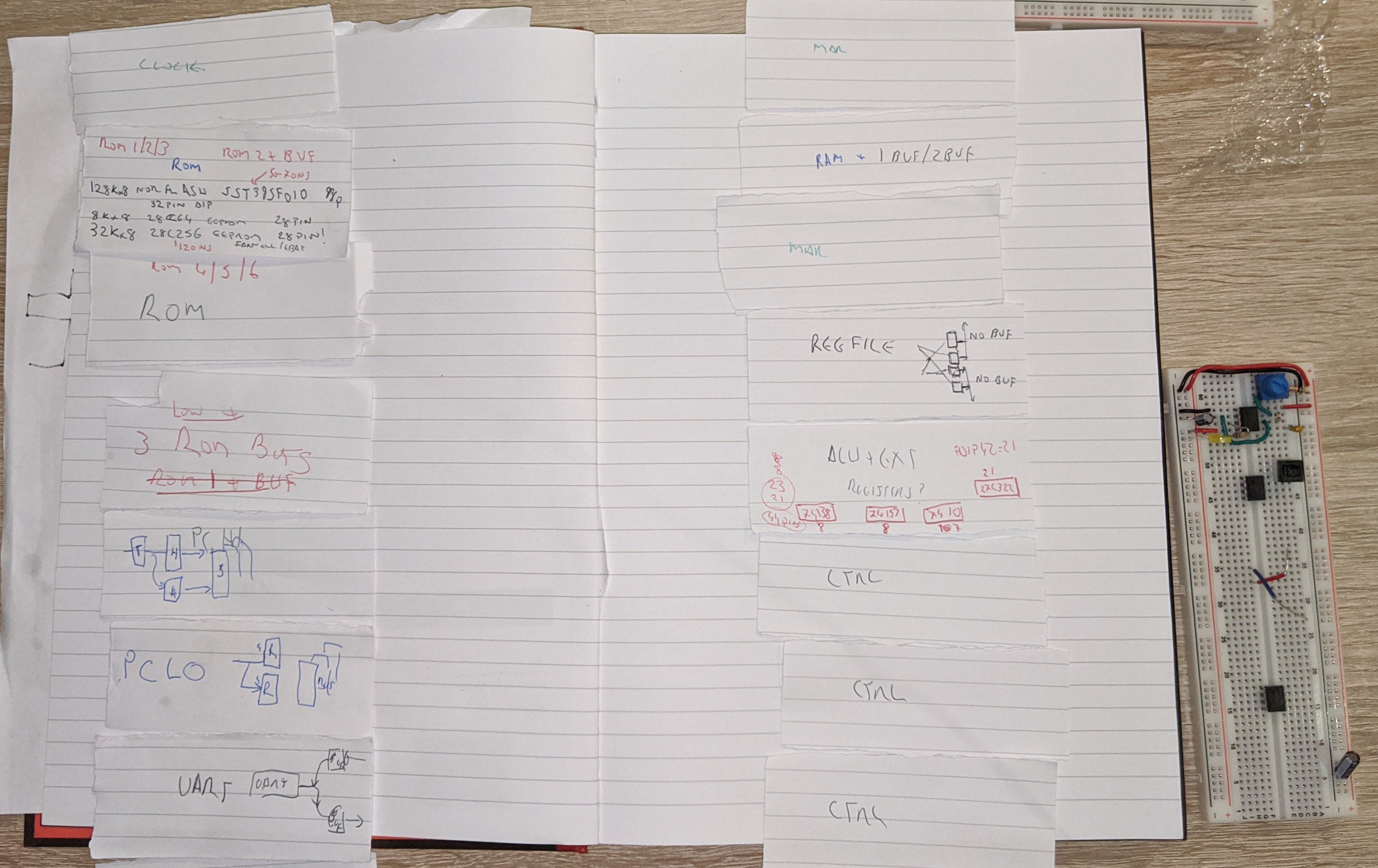
Program ROM and control logic module needs building as you can see in the photo below.
The "ROMs" I am using are flash devices SST39SF010 128KByte and I'll only use 64K. Detailed board layout to follow. May lead to moving the clock module to the right hand column. We'll see.
I also want to find space for an indicator block with 7 seg displays showing the 3 ALU busses at least and possibly PC address as digits. I have an idea to build some 8 bit parallel to dual 7 seg modules.

Original paper layout...
Discussions
Become a Hackaday.io Member
Create an account to leave a comment. Already have an account? Log In.