I spent a couple of painful hours trying to figure out why I was getting strange 1.3v signals on some lines that also weren't switching properly.
I was dealing with a 7402 NOR gate and as you can see below it's pinout is the opposite of basically every other logic chip I have in SPAM-1.
Without checking the schematic I'd assumed the 7402 had the more common pinout, so I'd connected output to outputs and inputs to inputs, which helps explain why nothing was working for me last night.
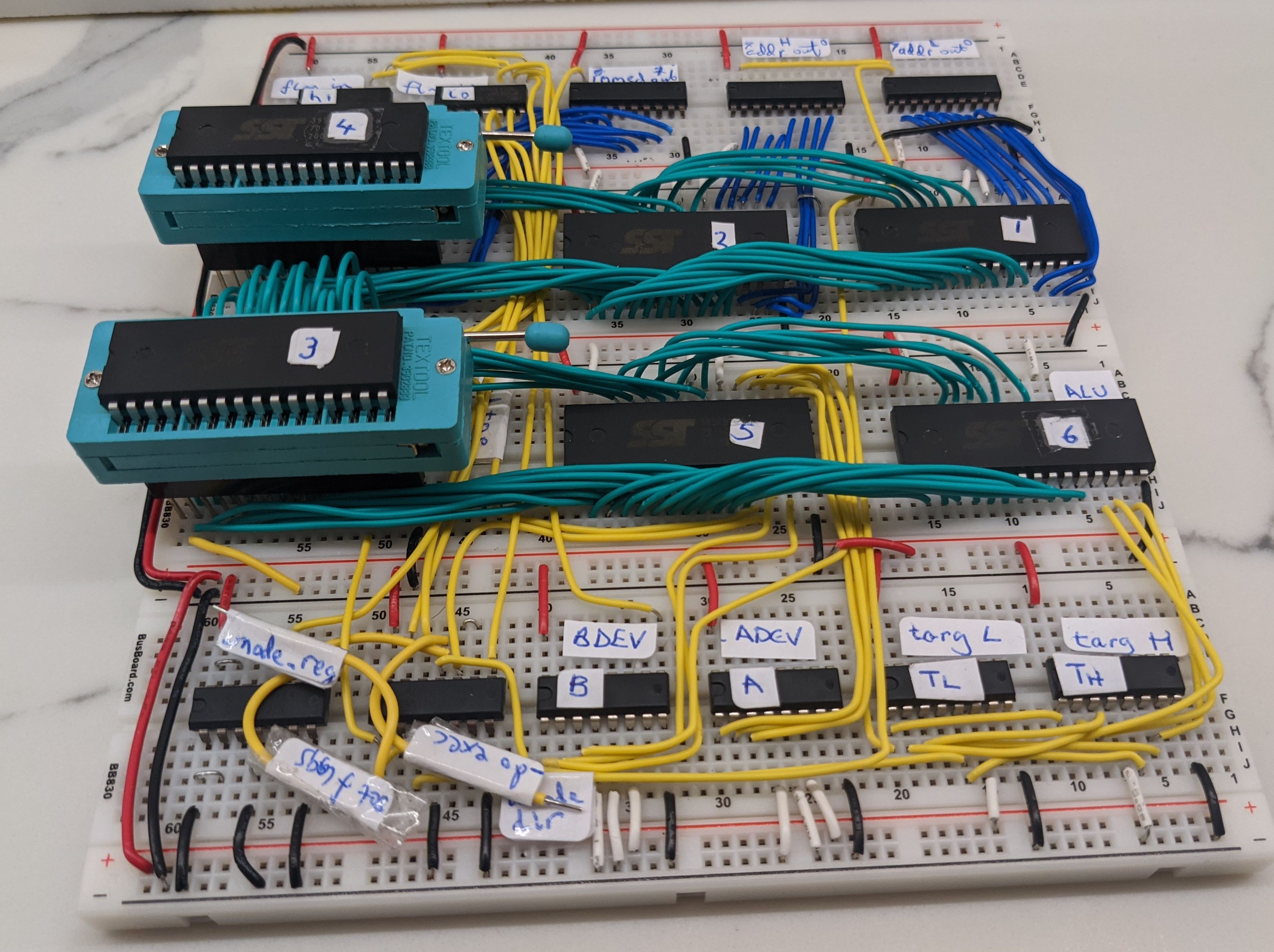
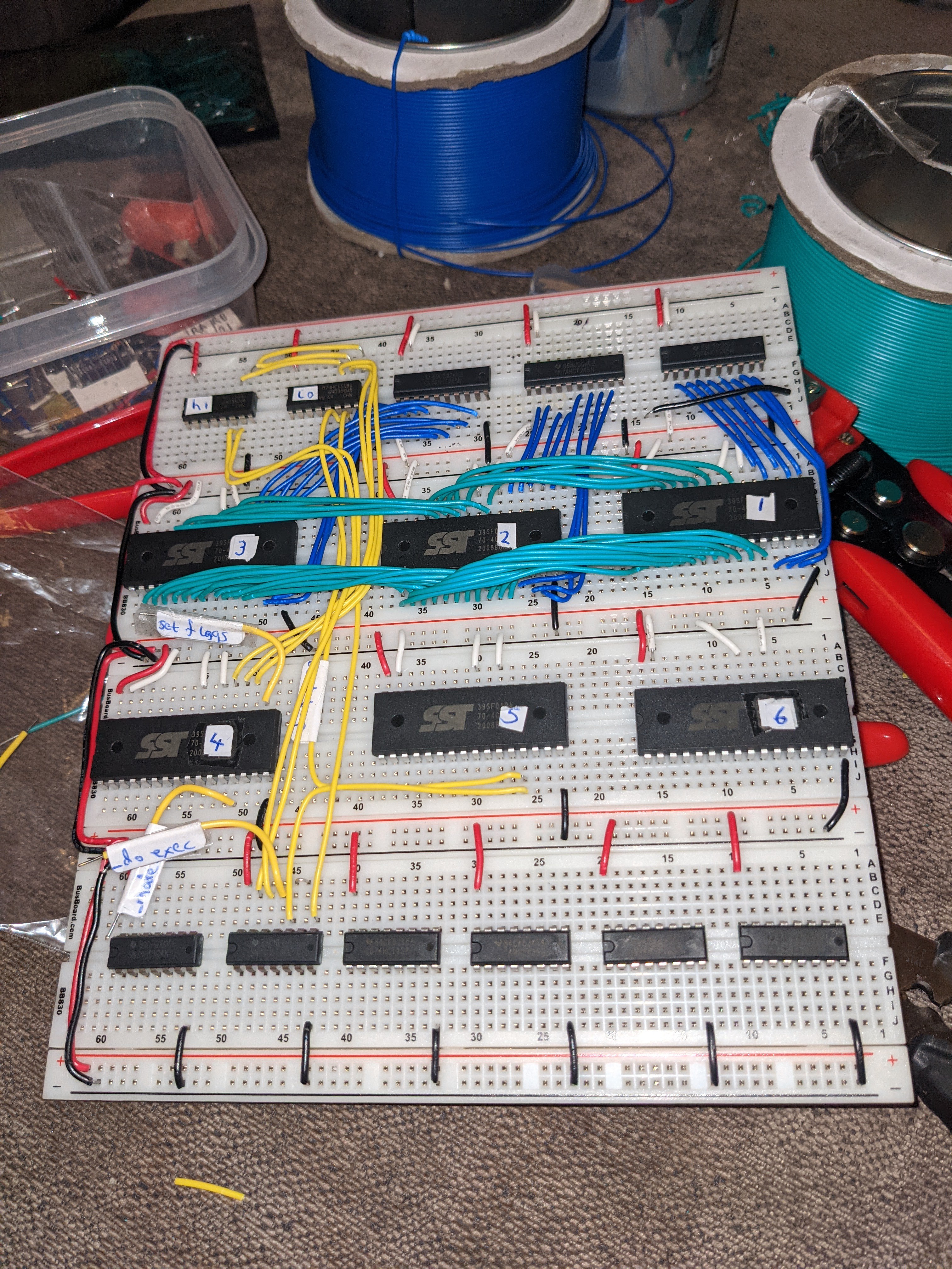
It recently executed it's first "hello world" program compiled from SPAMCC it's C-like high level language - this hello world responded to key presses on the UART stream by piping back "Hello World" to the serial monitor. At present SPAM-1 has no RAM or registers wired, though they are built as you will see in the latter half of this video on the rigth hand side. The lack of RAM/registers means SPAM-1 can't really do much else yet but this proves out that the control logic, timing, decoding and conditional instructions are working fine so far.
The hardware around the UART did something strange though - it printed random repeats of the characters I was sending back to the serial monitor. What was actually happening was that an oscillation was setup due to the combination of the gating of a UART /WE input signal with the UART TXE output signal, plus, the particular opcode that I was using to detect that it was valid to write. This feedback loop was easily fixed, however I was surprised (annoyed) because I'd not seen the same behaviour in the Verilog simulation so I went back and looked closer. I was even more surprised to see that I had forgotten that one of my existing test programs for the UM245R verilog model actually demonstrated and relied on this same oscillating behavior - which was comforting in a bizarre sort of way as it showed the hardware and model to actually match.
You will hopefully be aware that I have a complete behavioural simulation of SPAM-1 in Verilog (suggested by Warren Toomey aka Dr WKT) .
The simulation is as far as I can make it also timing accurate for the chips I've used in the hardware.
This paper above was instrumental in my understanding (a bit) how timing works in Verilog and helped me decide to go for a "Transmission delay" approach because that is most aggressive in highlighting glitches if there are any. My entire model hasn't yet switched over.
Really important for folk to understand if hoping to get the most from a model.
The conditional instructions in SPAM-1 are based on the various state flags; carry, negative, equal, greater than, data in ready, data out ready and so on.
With the exception of "not equal" all the checks are positive , eg "do exec if equal" , or "do exec if data ready"
I didn't realise before that this seems to lead to more code bloat than negative logic, eg "do instruction if data Not ready"
I found myself writing something like this frequently...
Top:

     If data is ready then jump to Handle:

     Jump to Top:

Handle:

     -- do stuff
With negative logic I get...
Top:

   If data not ready then jump to Top:

   -- do stuff
I don't know anything about research on this but is it the case that most of the time your design is better off with negative logic? Some CompSci person must know.
This is the kind of question I started this project to provoke.
Half of the CPU hooked up and then I realise there's no space for a single AND gate that I needed for the program counter. control logic.
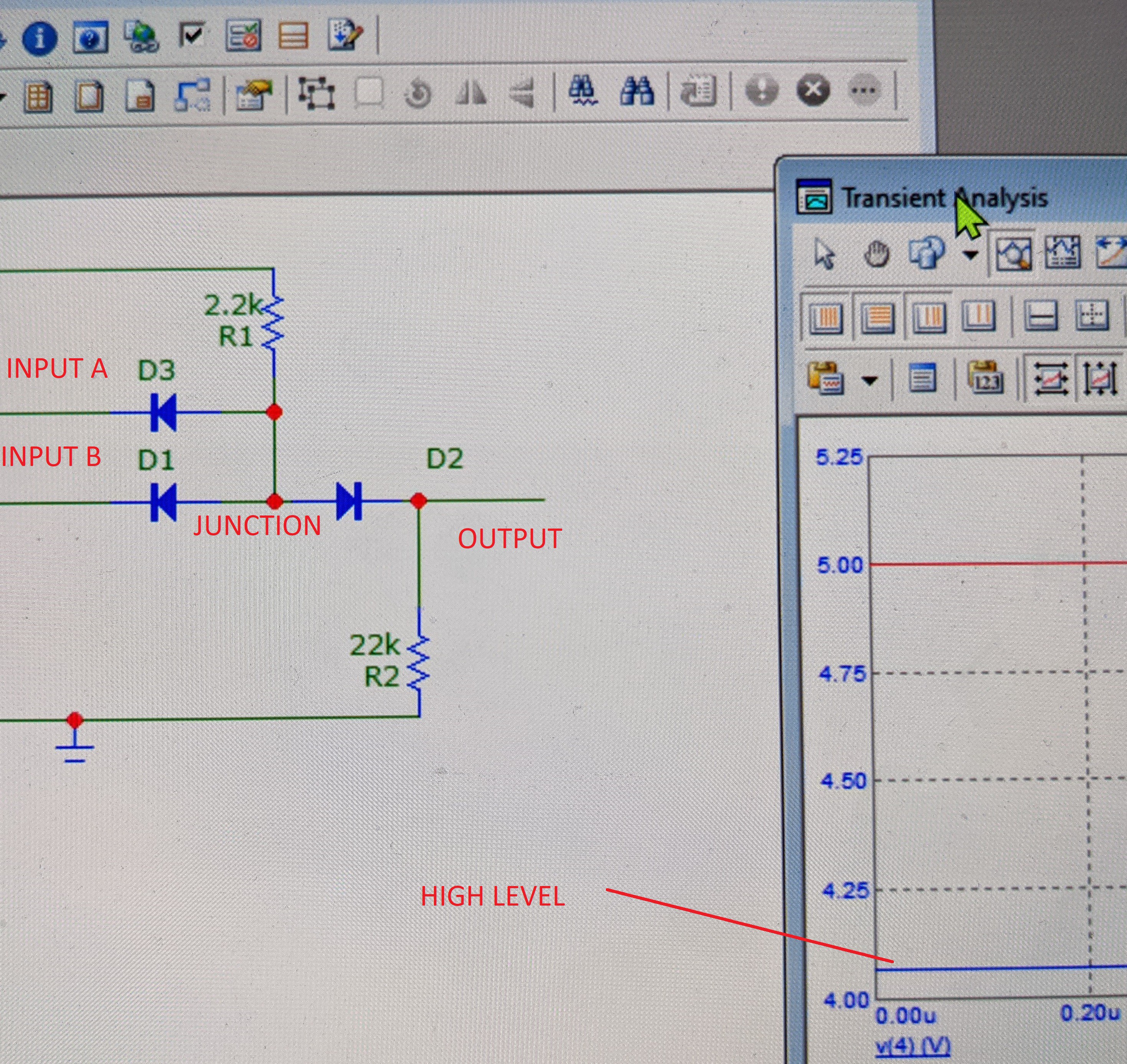
I needed a solution, then I realsed that I had some 1N4148 diodes decided to have a go at some "diode logic" to add some variation to the implementation. There was a tiny bit of spare space at the end of the control logic and so ....
I then simulated the AND gate it on (free) Microcap 12 as shown in the screenshot below to see how the logic levels would look. Getting a low of about 300mv and a high of over 4v I decided that it was sufficient.
D2 and D1 below are the AND gate inputs and the output is via diode D2. Reading the PDF again I think I now understand why the design I was looking at had two diodes in series at the out where below I have only a single diode D2. I think it's so that it is guaranteed that the forward voltage of the output path (ie D2) would be greated than that of the the inputs. I think was to ensures that the output is biased off properly when one of the inputs is low. It prevents any current flowing to the output. I'll see how it goes without it.
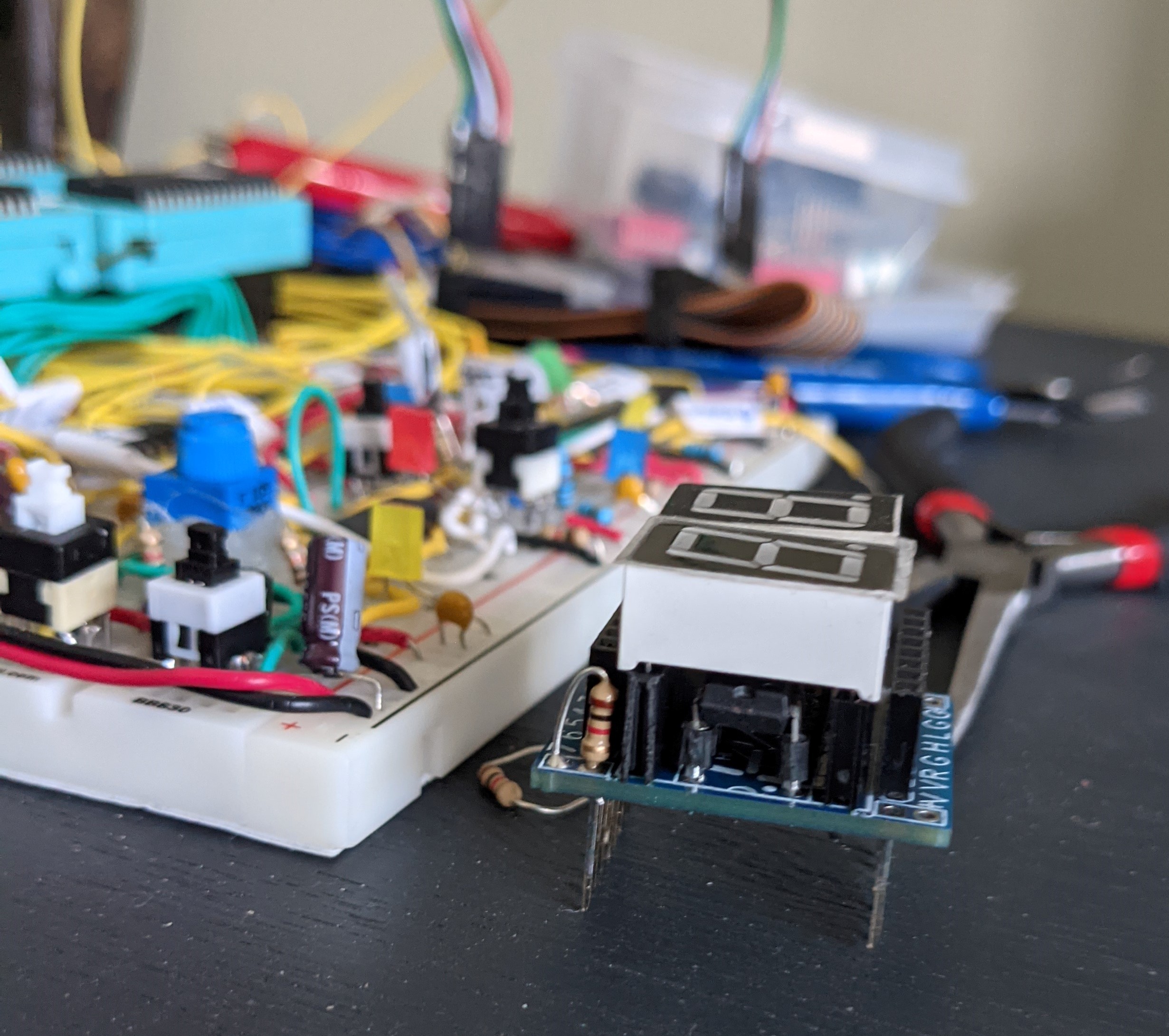
You can see the three diodes the two resistors crammed into three lines on the breadboard below.
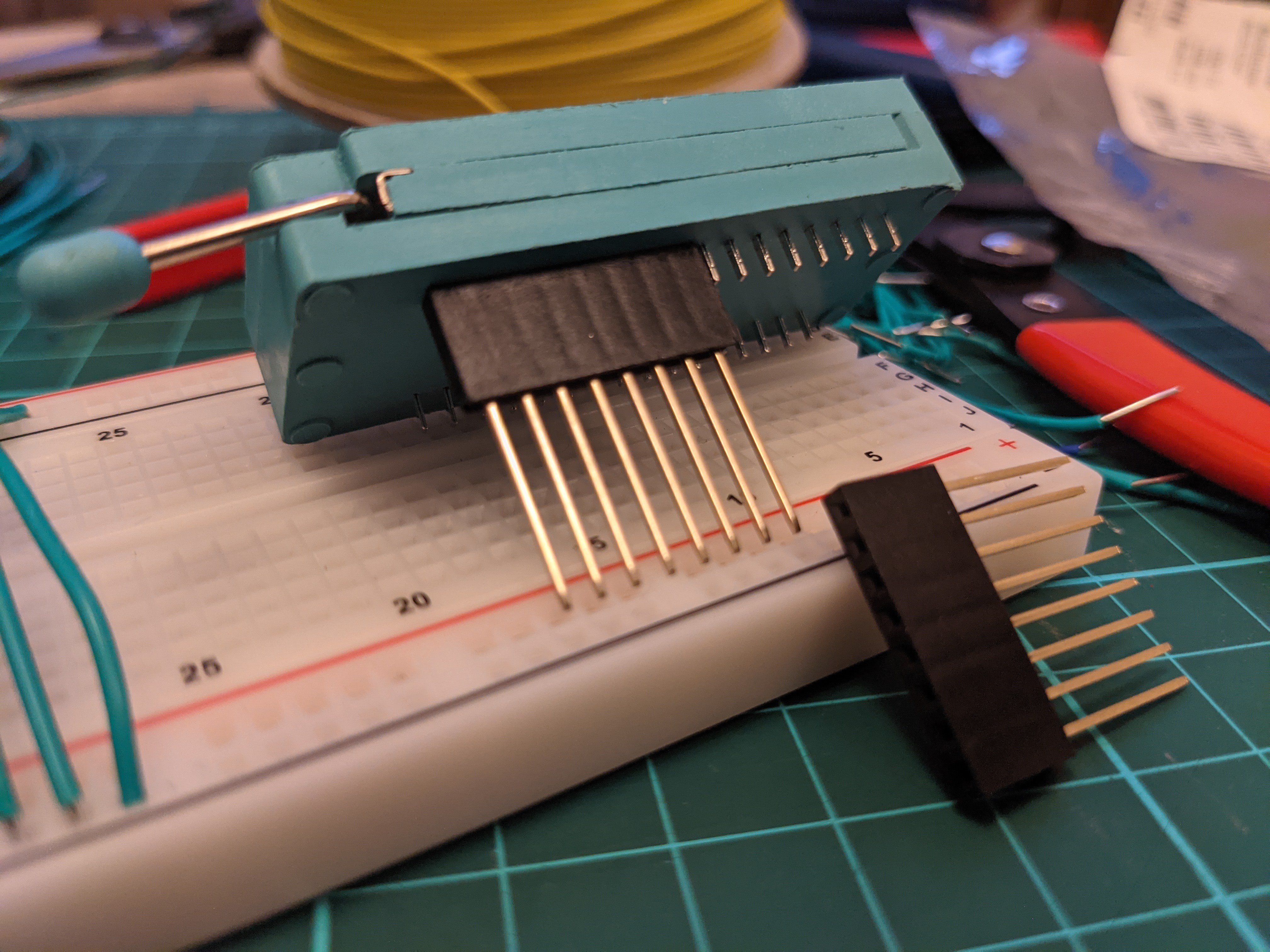
I was looking at my 32 pin ZIF sockets tonight and I noticed that while the pins are too short to be secure in a breadboard they were long enough to fit snugly into some extra long stackable female pin headers that I have.
This is such a simple solution to the two problems I had, firstly the problem mounting ZIFs securely in breadboard and secondly the need to get some clearance between the ZIF and the breadboard.
The clearance was needed to allow space for all the surrounding wiring.
I had 10 of the 8 pin headers but since I need 4 per device I just bought a bunch more of the stackable headers from the thepihut.com
These are an excellent length and the socket fits really securely and of course the breadboard fit it rock solid.
I now have clearance to run wires directly under the sockets.
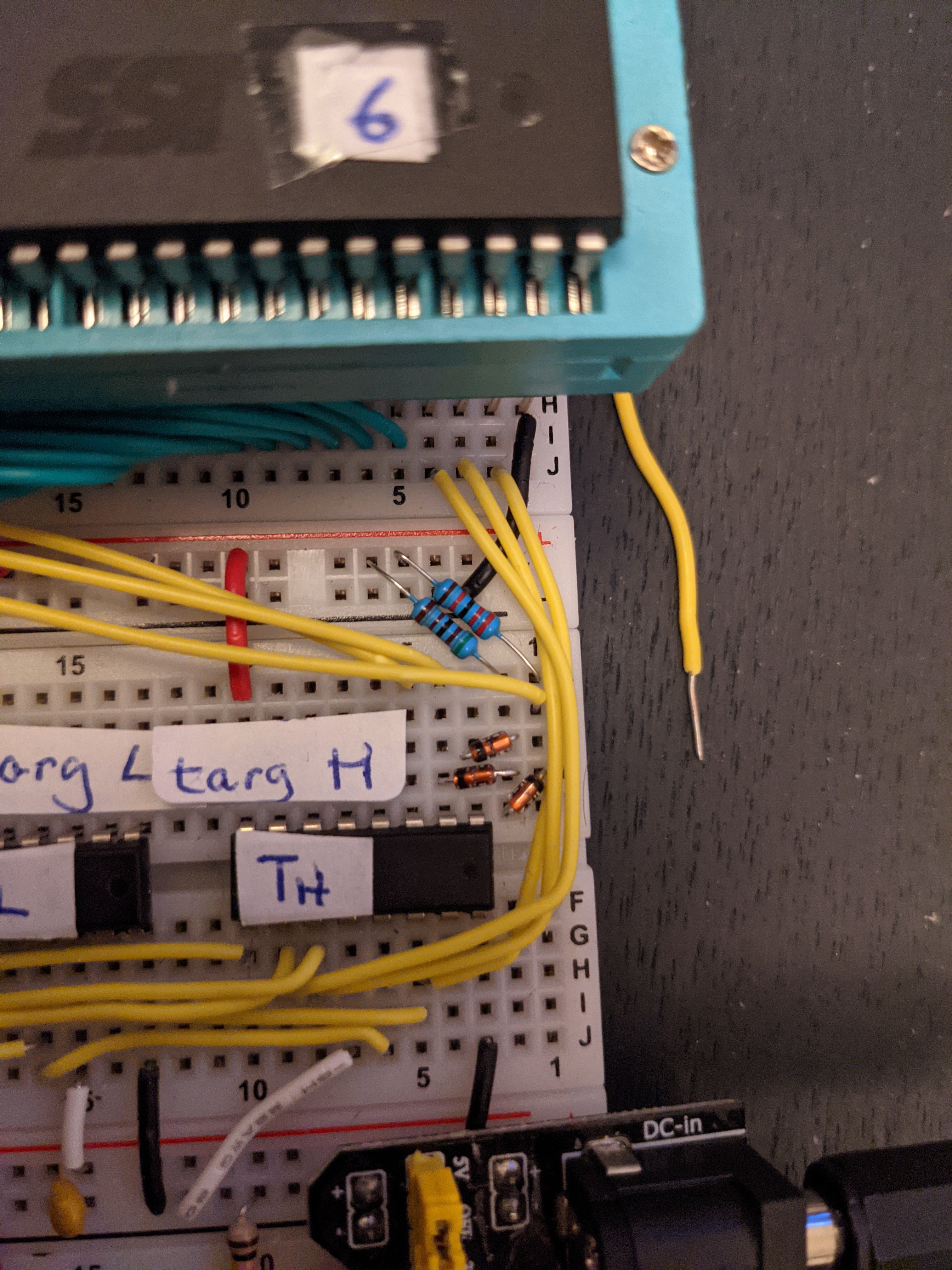
Finally getting progress again but not without setbacks. I had the ROM address lines all hooked up but then tore them out again today when I realised the next change I was about to make wouldn't fit.
I've decided to put the ROMs in ZIF sockets. But the existing chip position didn't leave enough space for the bigger footprint of the ZIF so I tore out the wriring and moved stuff around.
Even now the ZIF will not fit because it's wider footprint will collide with the wires. But I think I have fixed this with a trivial extender adaptor board for the ZIF so it sits proud of the breadboard.
The adaptor is https://hackaday.io/project/177325-zif-socket-adapter and the idea is that it puts the ZIF on stilts by using very long pin headers to attach to the breadboard. To be honest in retrospect this would have been pretty easy on veroboard rather than getting PCBs made up.
 John Lonergan
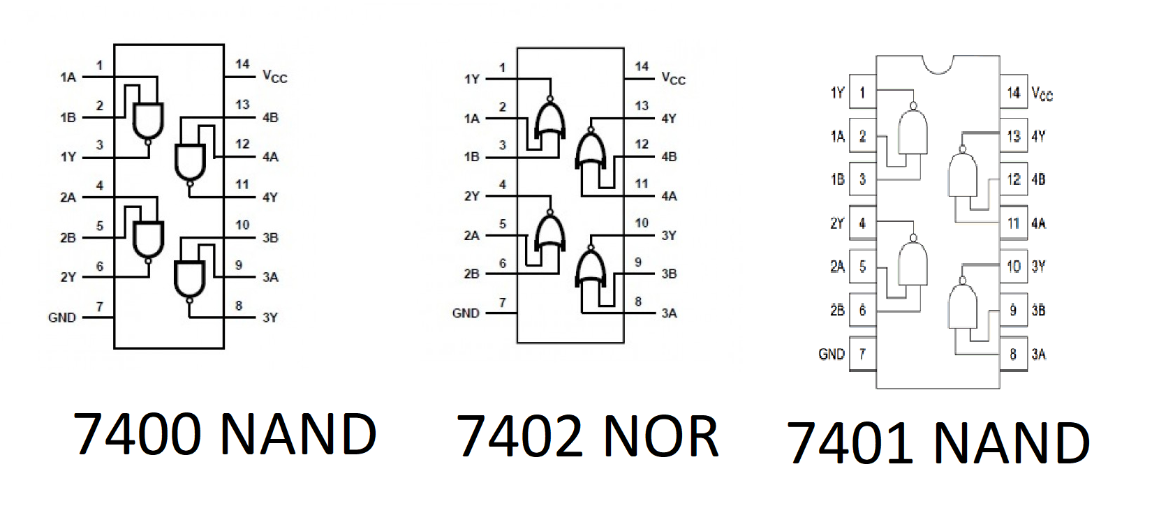

 (Spot the iwiring mistake)