 furrysalamander
Found it ready to go into the trash can, and brought it home.
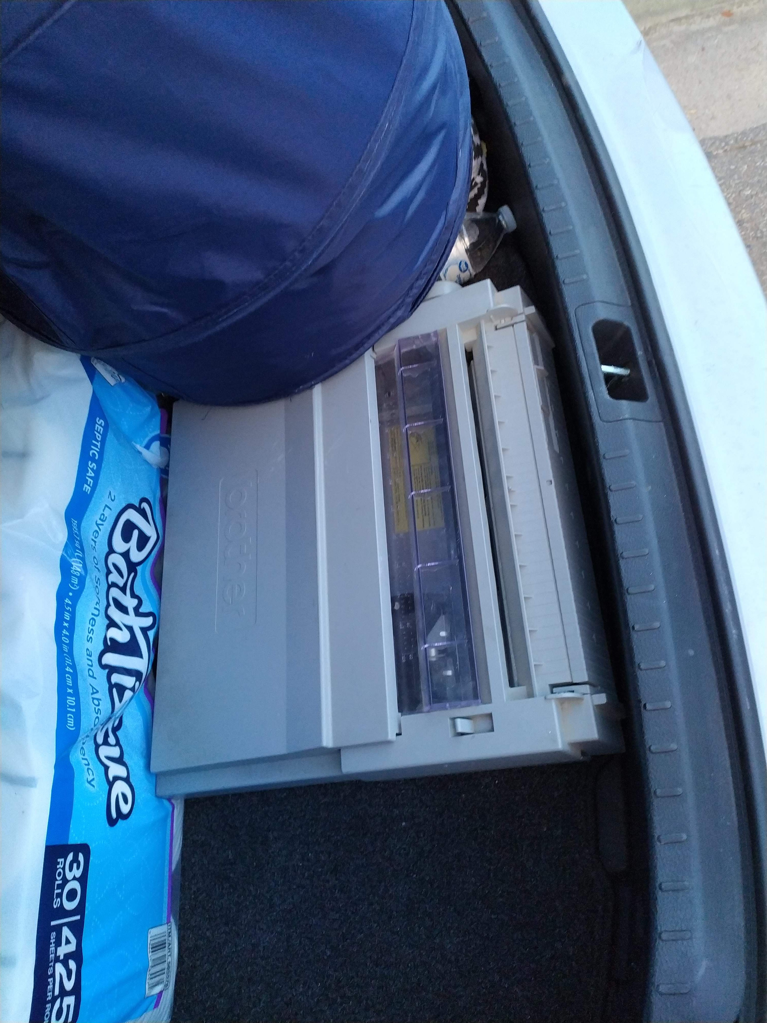
Not too much to go on yet, but I've already got it pulled apart. Much to my surprise, we have quite a bit to work with.
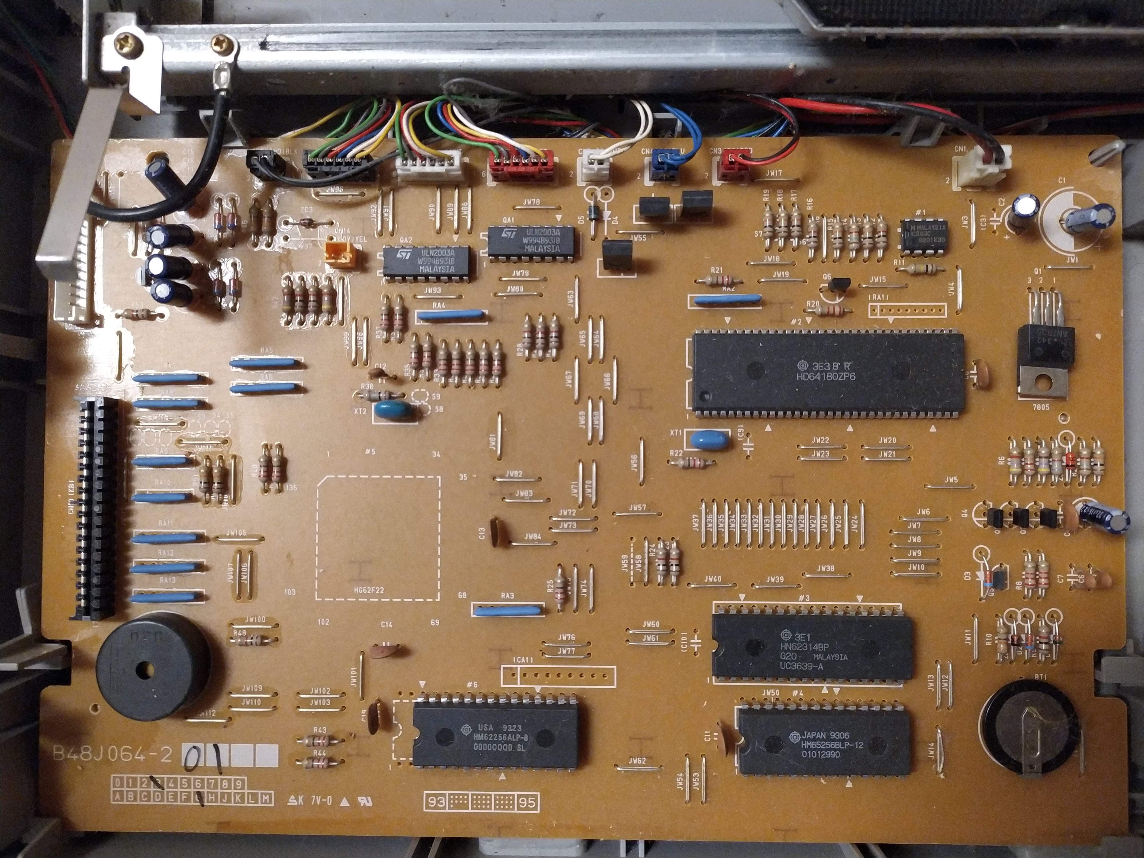
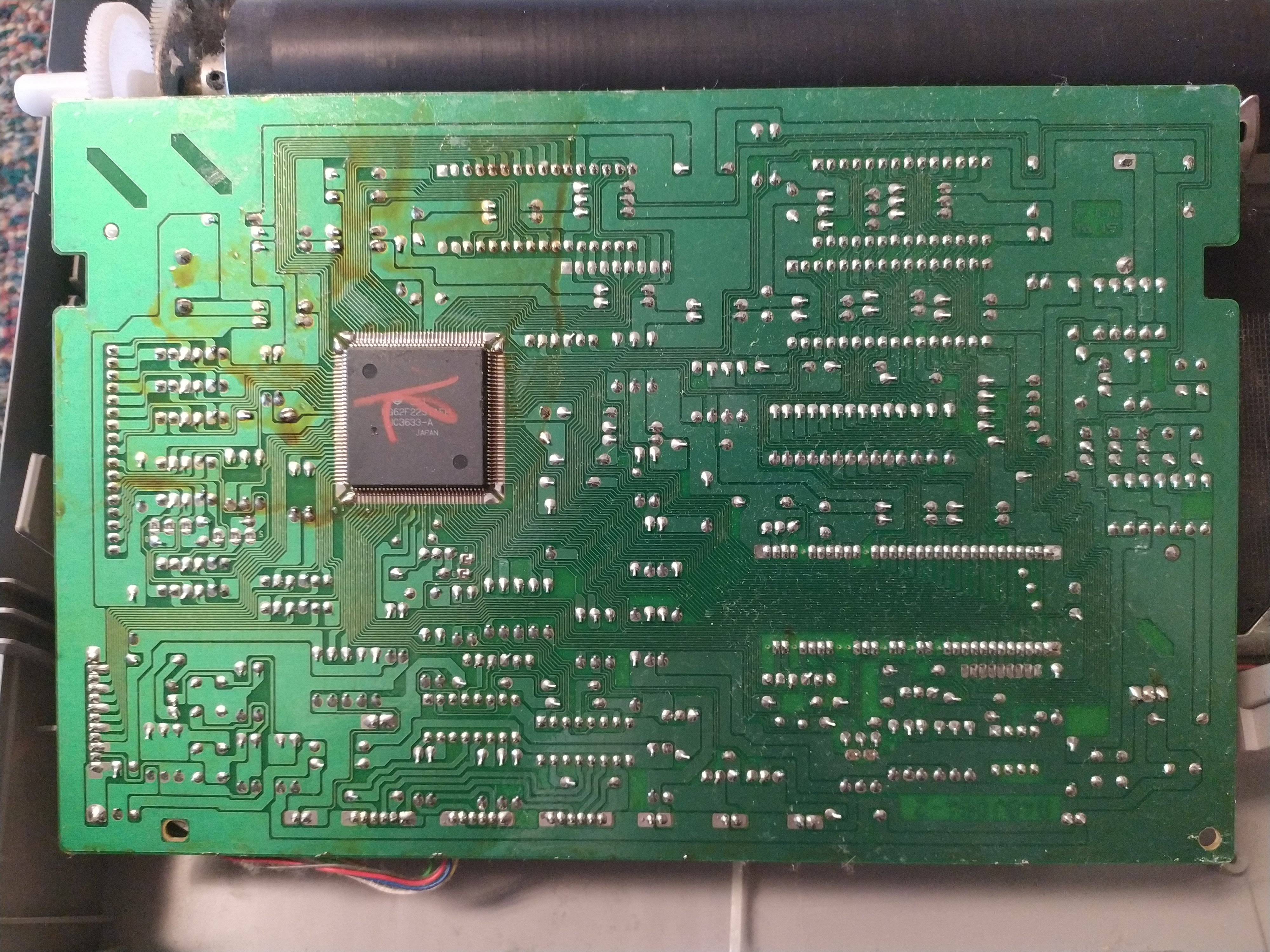
Here's a few shots of the interior.
Front of the PCB:
And the back:
Upon closer inspection, we have a few interesting chips on the front side.
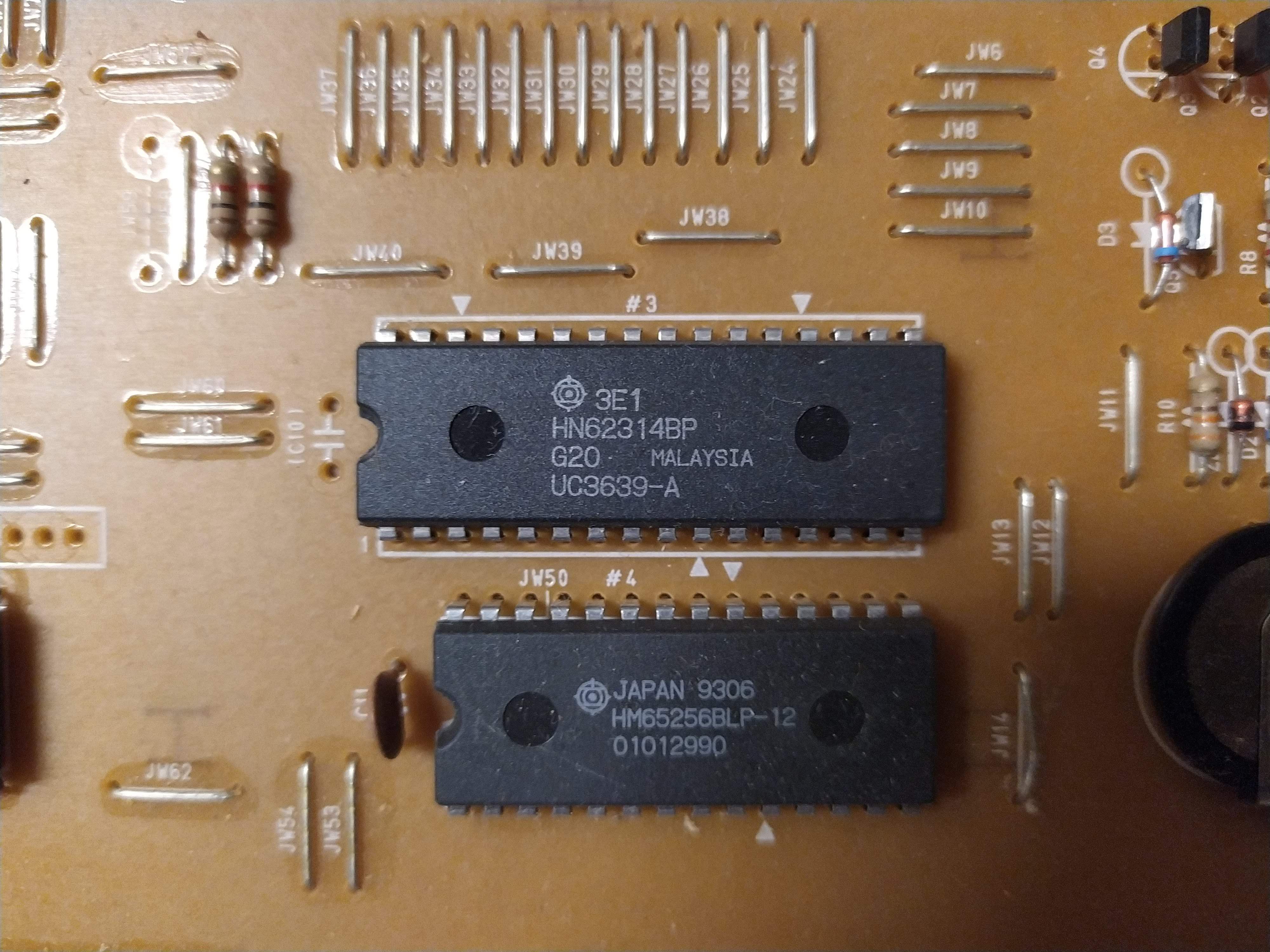
On top we have the HN62314B.
According to the datasheet, this is a mask ROM. I'm guessing this is where the program data is stored. Not reprogrammable, but luckily, I found a flash chip that has almost the exact same pinout.
http://ww1.microchip.com/downloads/en/DeviceDoc/20005022C.pdf
Main difference is the write enable line. Should be an easy enough fix.
The chip on the bottom appears to be RAM (HM65256BLP-12).
I'm not sure what part this play in all of this, but there's another RAM chip to our left (HMG2256ALP-8):
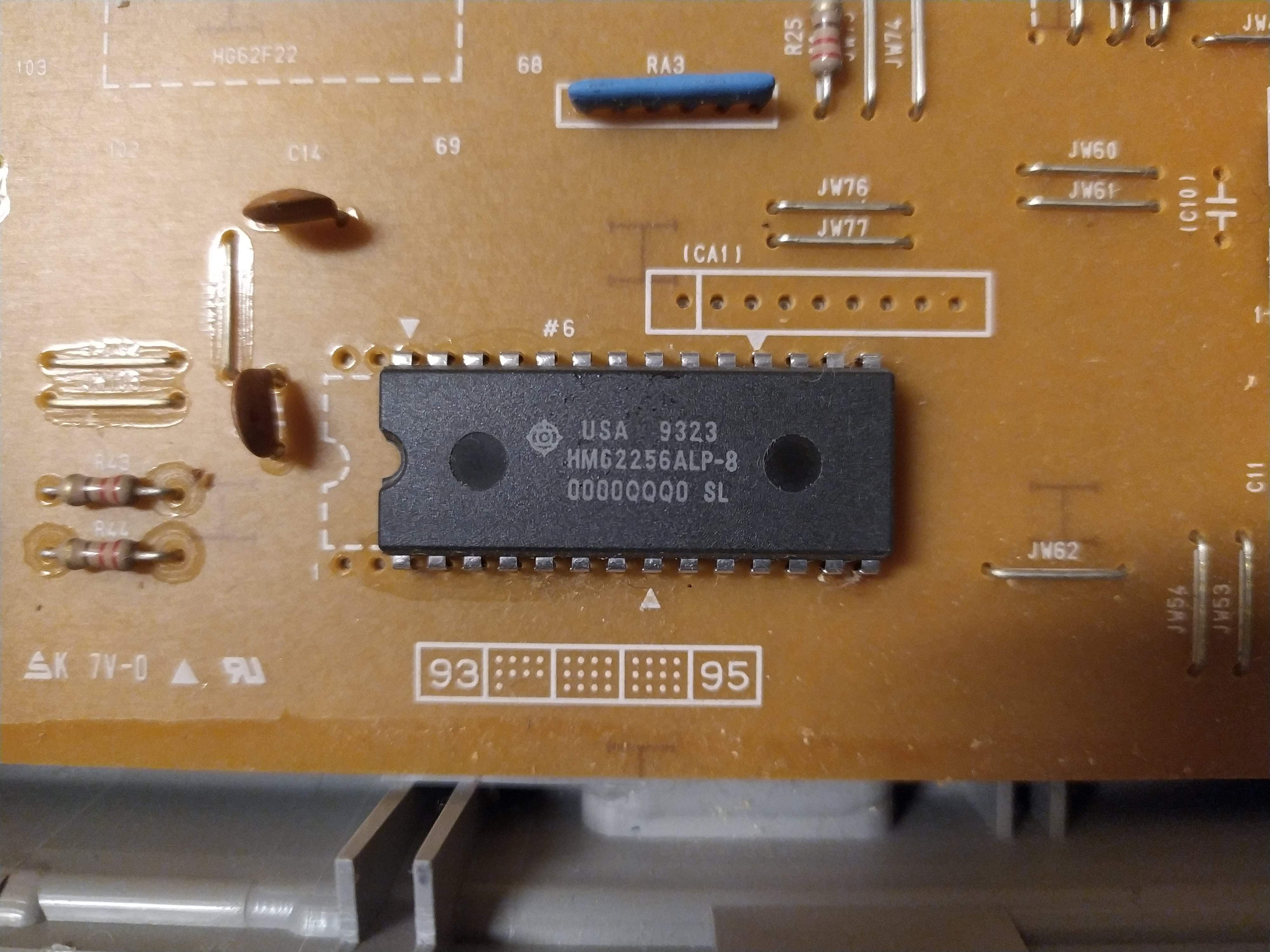
I'm guessing that one of these acts as the persistent storage. There's a coin cell battery on the bottom right corner that probably keeps the data loaded when the power's cut. Probably pretty dead at this point though, so I can't imagine that the persistent storage lasts very long.
That's about it for this log, but I'll share more exciting things in the next ;)
Discussions
Become a Hackaday.io Member
Create an account to leave a comment. Already have an account? Log In.
I doubt if those static RAM chips are used to hold persistent settings. Their quiescent current, while low, would still drain any coin cell too fast. Also they are far too large (32kB) for a few configuration settings.
Are you sure? yes | no
Probably not for configuration settings, but it can save the documents you type up. That would be in line with the 32KB. It also struck me as interesting that there were two chips. Will be interesting to see what I find out when I hook up the logic analyzer.
Are you sure? yes | no
Maybe one SRAM for program working area and one for documents. One slot seems designed to take 32 pin SRAM so may be expandable.
PS: 👍 for recycling.
Are you sure? yes | no