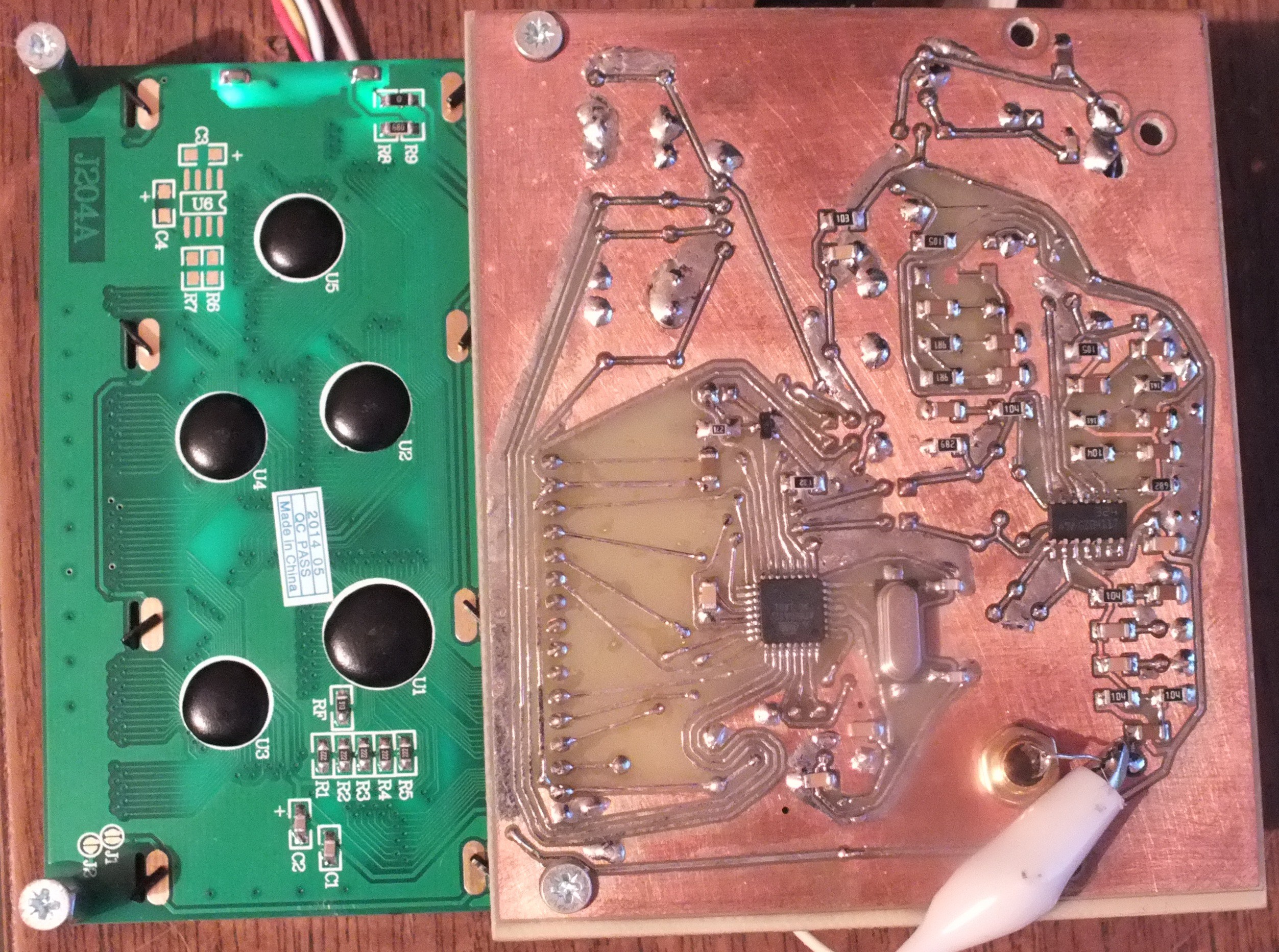
I soldered all the parts. The layout of the board is terrible but it works.
Some notes:
- LCD connector is soldered upside down due one-sided PCB. The final version will be soldered on another side of the PCB.
- Trimmers are placed randomly. Not easy to find which does what. Too many trimmers and jumpers. I plan to simplify the input filters and reduce the number of these jump&trim.
- Optional (and different) connectors for audio input (e.g. 3.5mm socket) and power (e.g. small screw terminal block) would be convenient.
- Bad footprint of power connector.
- USB->serial chip on board (e.g. PL2303) would help with the external connection
So, looks like a list of several small improvements for the next version of the PCB :)
 CrazyChip
Discussions
Become a Hackaday.io Member
Create an account to leave a comment. Already have an account? Log In.