custom bldc motor board using fpga
custom pcb for controlling a bldc motor optimally
custom pcb for controlling a bldc motor optimally
To make the experience fit your profile, pick a username and tell us what interests you.
We found and based on your interests.
For FOC we need to measure the current flowing in our motor windings. The drv8323 chip supports this by adding shunt resistors on the low side mosfets as can be seen in the datasheet:
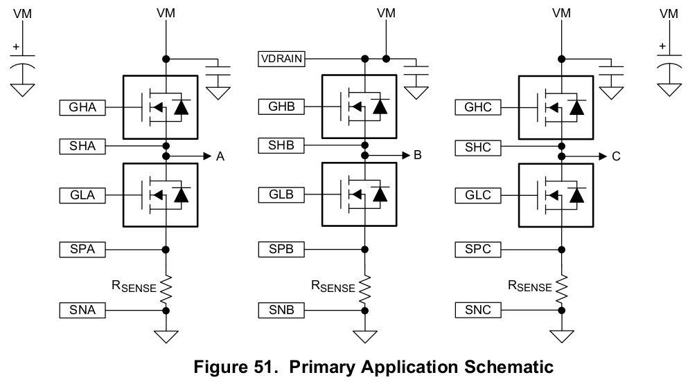
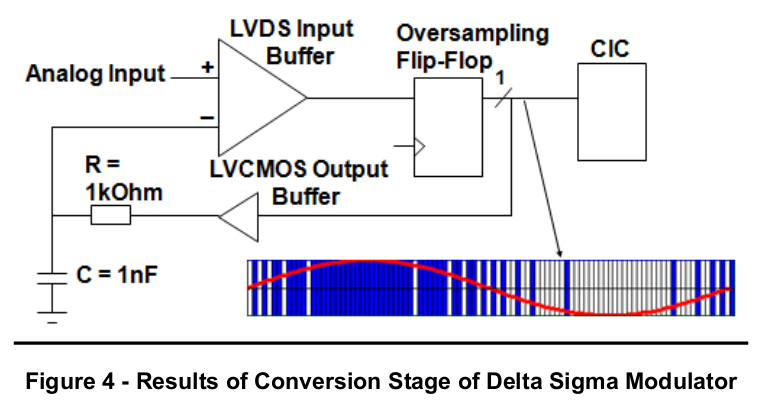
The chip internally amplifies the signals and provides an analog representation on the SOA, SOB, SOC pins. This means, we can get the current more or less for free by adding the shunt resistors. The only downside is, we need an adc. The iCE40lp8k doesn't have an adc, but lattice provided a beautiful paper, explaining how to make your own, using the lvds pins of the fpga. All you need for this, is a simple RC network and in addition to one lvds pair, one more pin for tracking the voltage:
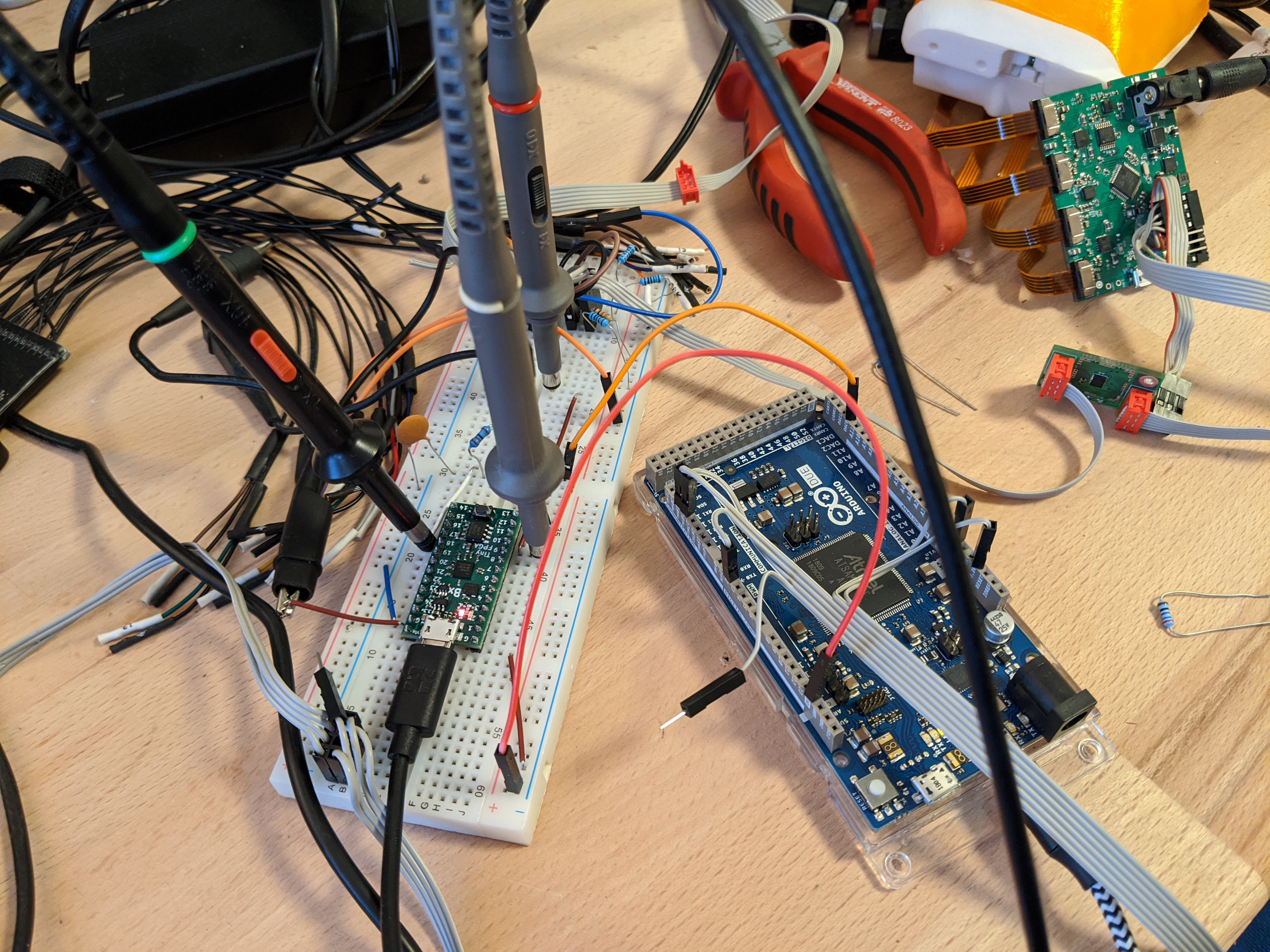
To test our adc we are using an arduino due and its' dac to produce a voltage waveform. You can find the sketch here. The code running on a Tinyfpga-BX is very simple, you can find it here. We didn't have the cap and resistor values as recommended in the datasheet. In this setup we are using 1.8k and 220nF:
The fpga is able to track the voltage quite well, within a certain voltage range:
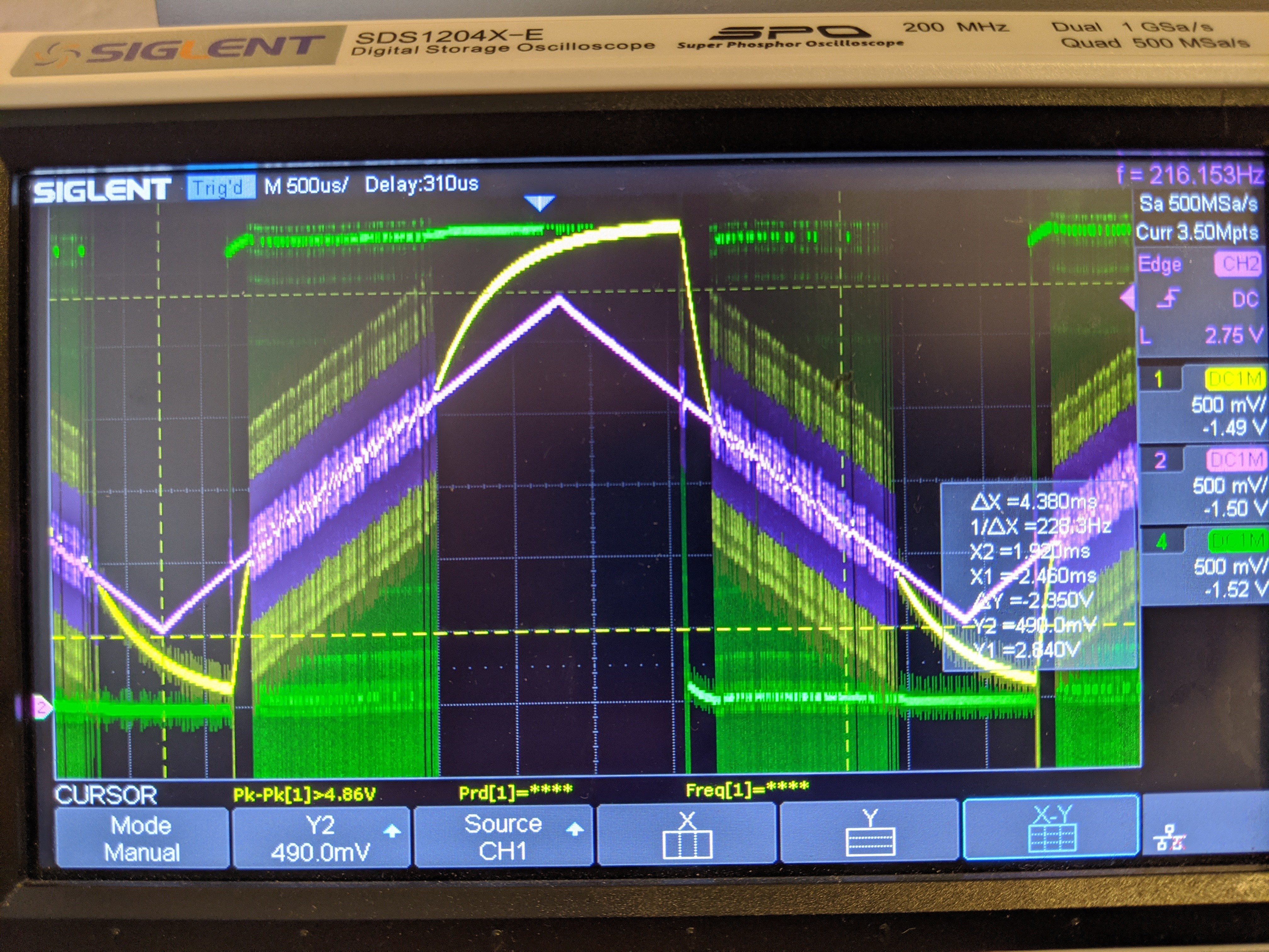
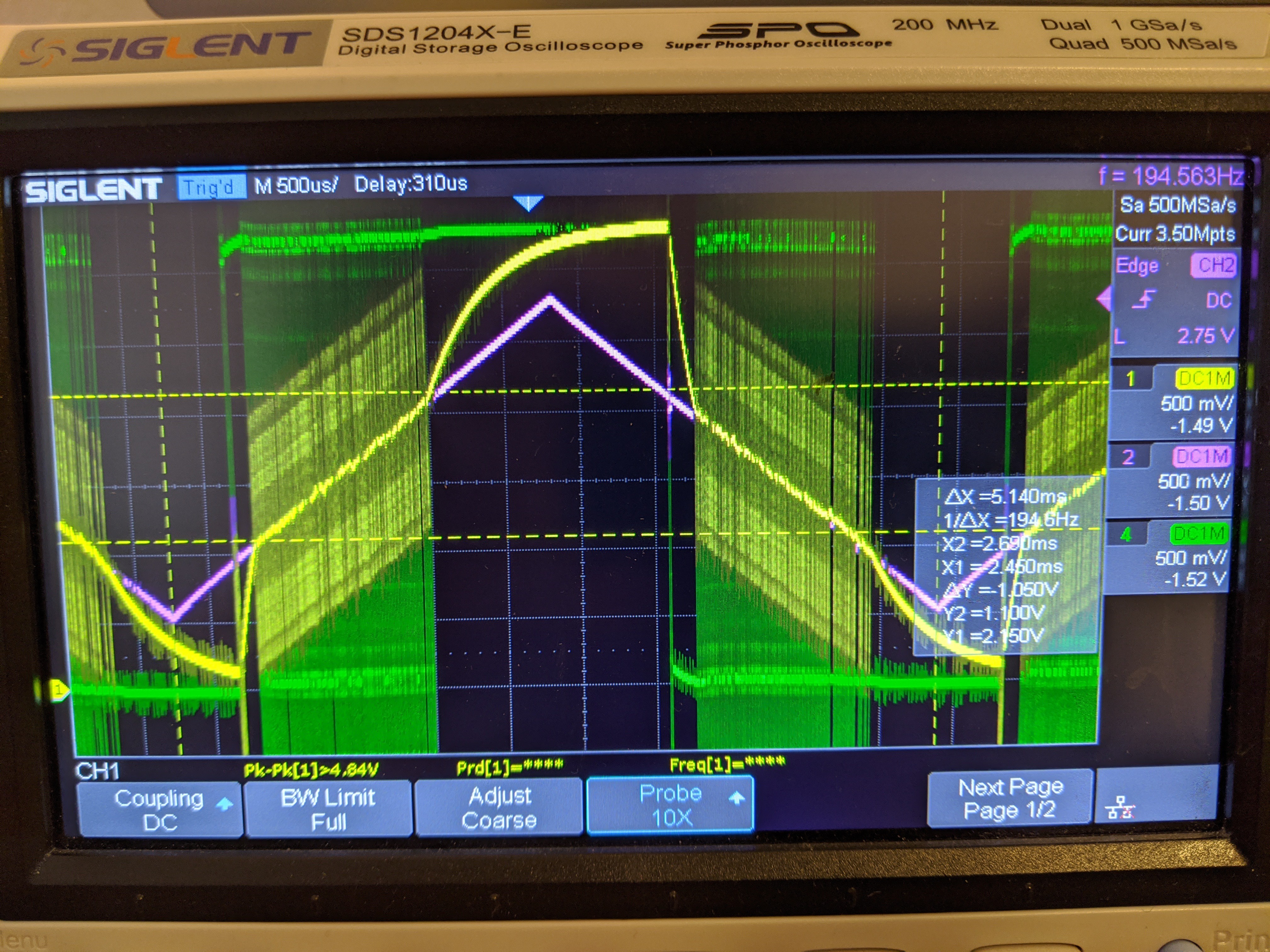
In the picture above, violet is the target voltage coming from the arduino due. It's just ramping up and down between 500mV and 2.8V at around 200Hz. Yellow is the output of the RC network and green is the LVCMOS input into the RC network. As you can see, the yellow line is able to track the violet target voltage quite well, between 1.1-2.1V:
And I think this is related to the LVDS specs, as taken from the ice40 family handbook:

So the max voltage for the lvds input is 2.5V and there is also a differential input threshold given, typically 350mV. So this means that the lvds pins will detect a difference between each other only above 350mV. This might be an explanation why the fpga looses tracking in these areas. And also why the tracking voltage oscillates so much around the target voltage. The tracking voltage overshoots within the differential input threshold voltage band.
To get a digital value, representing the voltage level, the green PDM (pulse density modulation) signal needs to be converted. Lattice recommends a CIC filter in their paper and I remember dealing with a similar conversion problem when working with MEMS-microphones. In the following picture you can see, how the green PDM signal density goes down with the voltage. This change in pulse density encodes our voltage level.
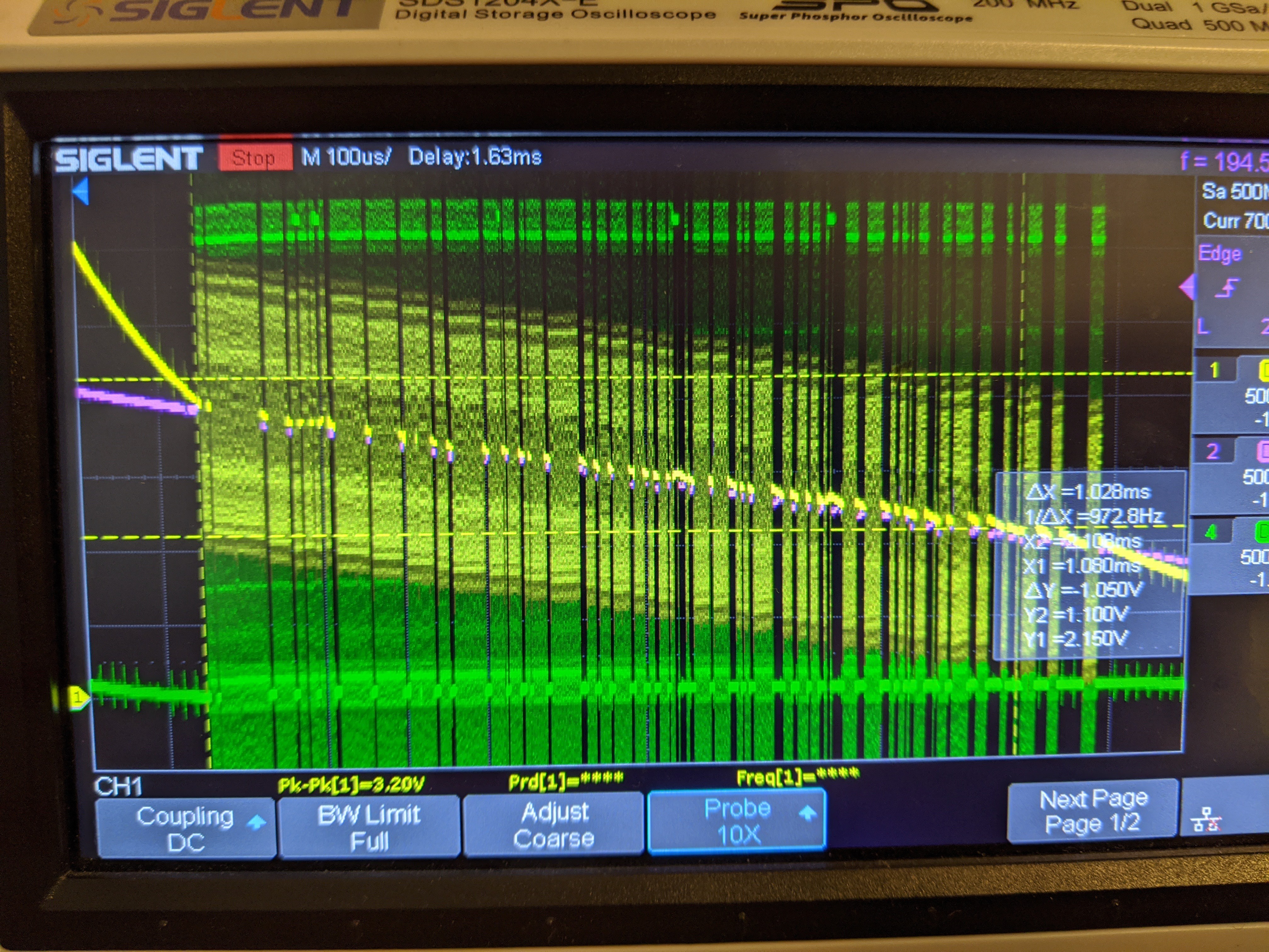 Before we go down the rabbit hole of digital filter design (eg following a guide like this)...The PDM signal can be converted simply by adding the PDM signal within a certain window. We chose a 256 clock tick window for the integration, because this allows the generated 8bit value to be conveniently send via uart. The arduino due was used to forward the uart data via ROS and was then plotted in rqt_plot:
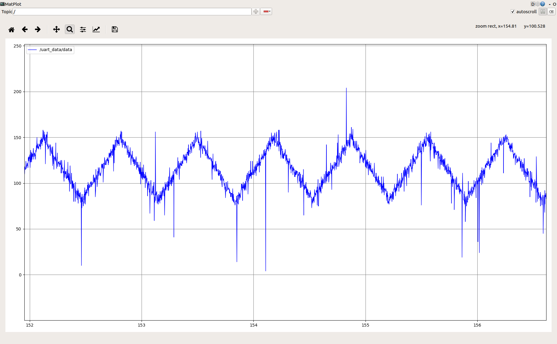
As can be seen in the plot above, the integrated value represents the voltage level. It is quite noisy and only valid within the valid voltage range, but not so bad for starters.
The icebus can also be used with non-fpga devices. For this we created a USB adapter with a ftdi USB->uart->rs485 mechanism and a rs485->uart adapter:
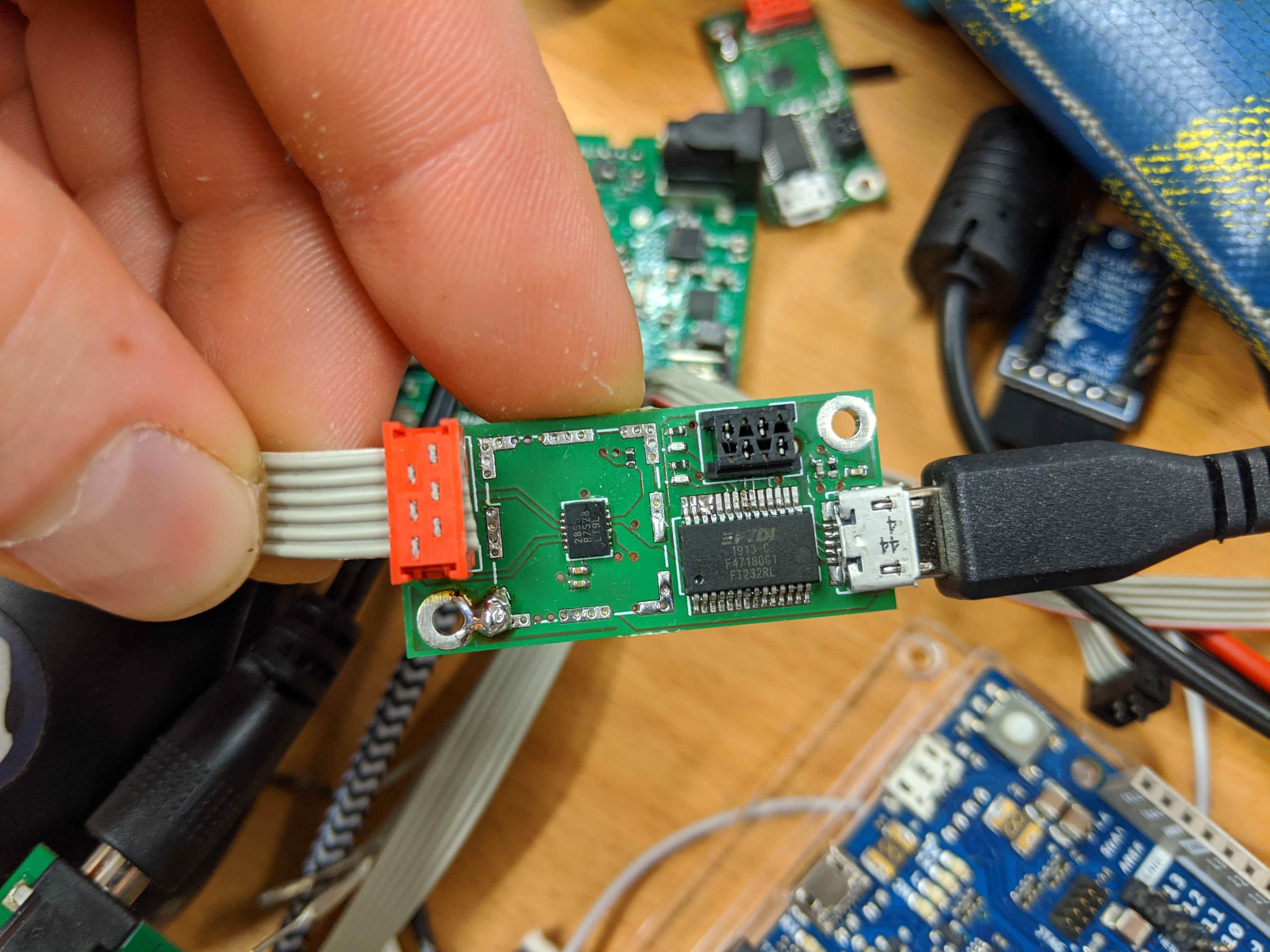
On the slave side you would either integrate the rs485 chip on your pcb or use an adapter that converts the rs485 signal back to uart:
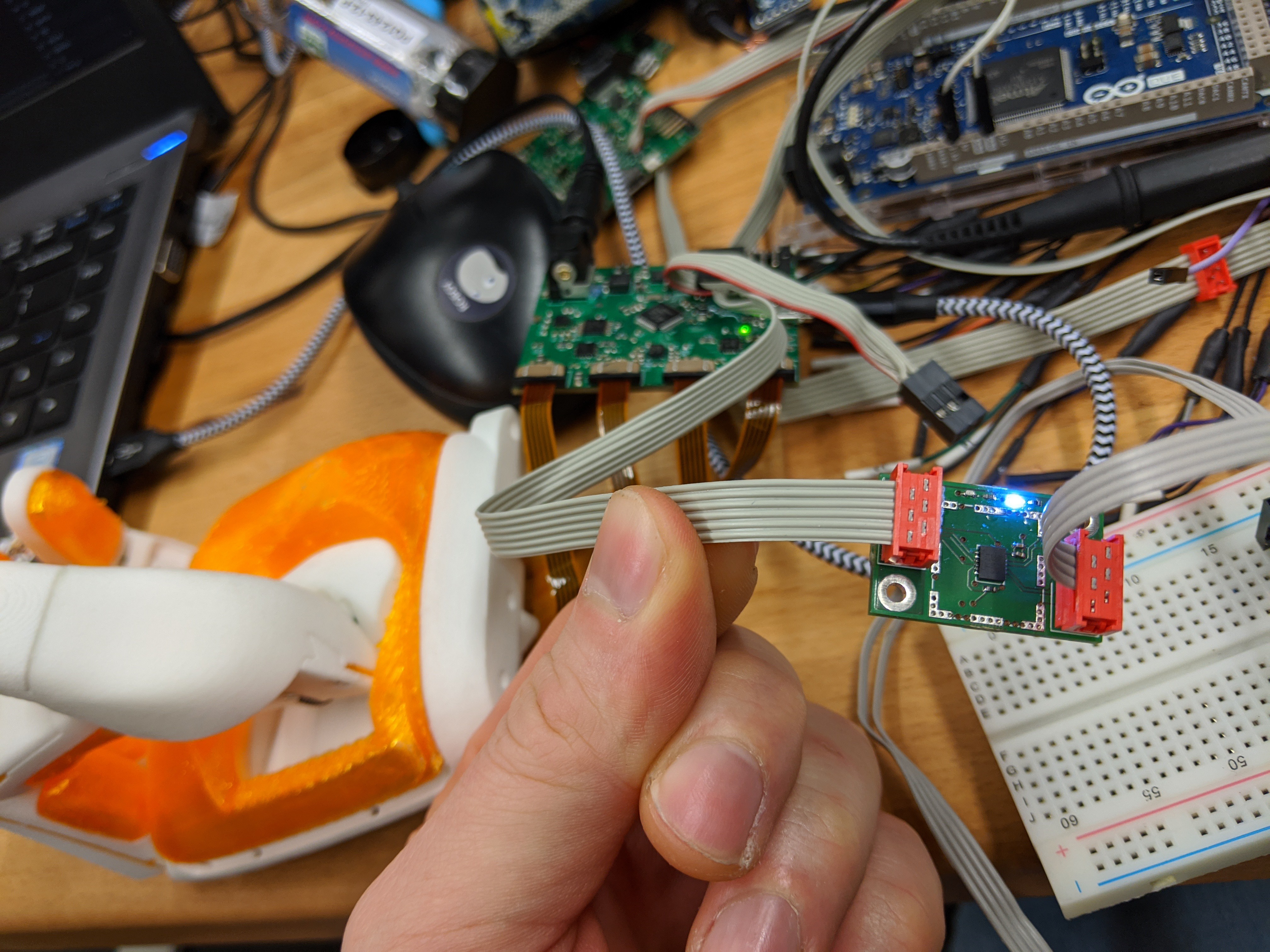
We have written a ros node that implements the icebus protocol using linux termios to interface with the ftdi chip. In this case it controls an openbionics hand, which runs on a samd21 arduino sketch. Of course you can't run the same speeds as with a fpga. The upper limit for the samd21 seems to be a baudrate of 19200. This gives you around 100Hz communication frequency for controlling the setpoints of the four motors inside the hand.
And here the hand in action:
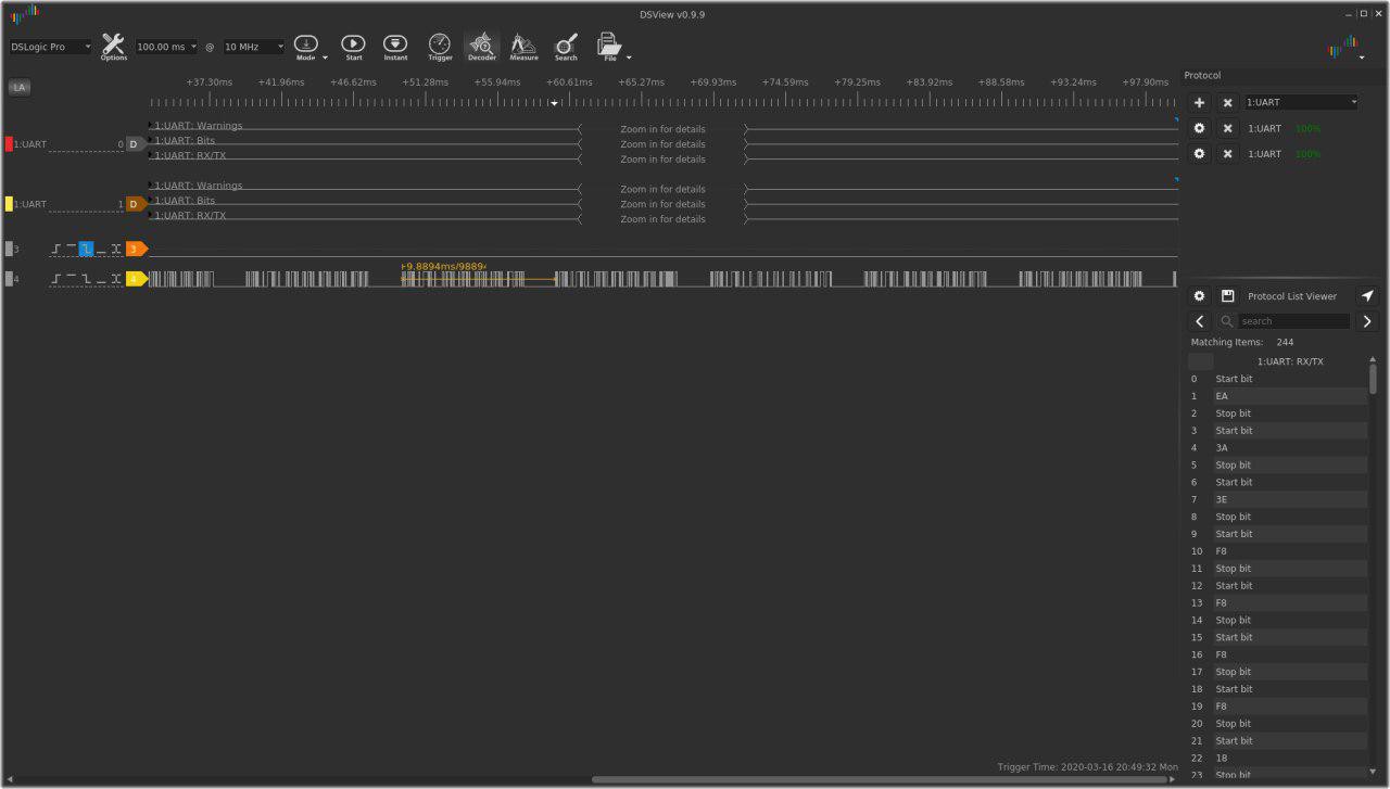
Here is a logic analyzer capture of the command frames:
For testing v0.7 we conducted two tests. The first test was to do 10000 cycles of lifting a 5kg weight up and down. The iceboard here controls the bldc motor mounted in one of roboy 3.0 muscle units.
The white dyneema tendon is rolled up by the bldc motor on a 12mm winch. The 5kg weight is lifted two revolutions of this winch within 1 second then lowers the weight to the start point within 1 second. This completes one cycle.
A FLIR TG165 was used to measure the heat distribution on the iceboard. The drv8323 chip and the low-side mosfets are the hottest components at around 40C.
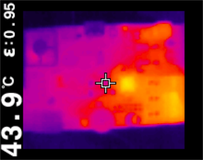
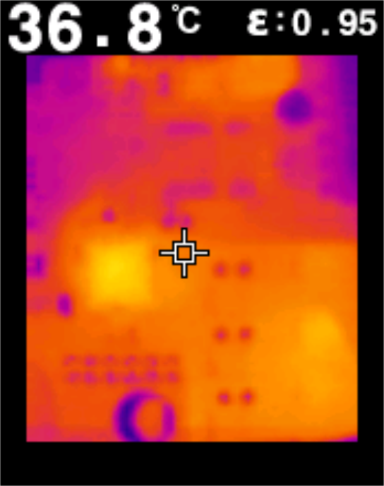 The second test was 10000 cycles of rolling up the tendon three times, within 2.5 seconds, then going back to 0 within 0.5 seconds:
The motorboard showed no signs of degradation after these tests.
The following image shows an overview of the components used in v0.7:
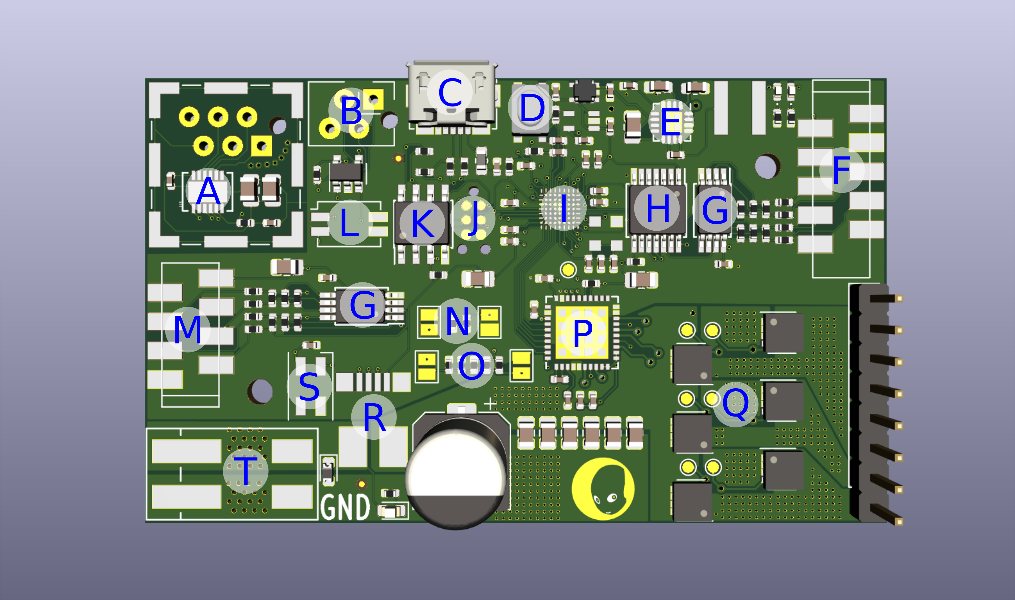
The following section gives some details about the motor control code.
We are using the Texas Instrument drv8323hrta chip in independent mode. This means we have full control over the mosfet gates. Commuting the phases seemed trivial at first, but as it turns out, you need to know the specs of your mosfets really well in order to do this right. The key word here is dead time insertion. It essentially refers to the mosfets not being ideal switches and not turning on or off instantaneously, but with a certain delay. When we commute the phases, we have to be sure the opposing mosfets are closed, otherwise you can easily burn your mosfets by shoot through gate states. One common way is to use dead time insertion. The exact timing can be calculated from the specs of our mosfets, and I will make a mental note now to do that later. For now we are just using an arbitrary large enough dead time. For our application the motor spins quite slow and the big dead time will be really only noticeable at high motor speeds. Here is the code that handles our bldc commutation:
always @(posedge clk16MHz) begin: BLDC_COMMUTATION
   commutation_state_prev <= commutation_state;

   if(commutation_state!=commutation_state_prev)begin
     dti <= 1;
     dti_counter <= 1024;
   end

   if(hall1 && ~hall2 && hall3)begin
     commutation_state <= A;
   end
   if(hall1 && ~hall2 && ~hall3)begin
     commutation_state <= B;
   end
   if(hall1 && hall2 && ~hall3)begin
     commutation_state <= C;
   end
   if(~hall1 && hall2 && ~hall3)begin
     commutation_state <= D;
   end
   if(~hall1 && hall2 && hall3)begin
     commutation_state <= E;
   end
   if(~hall1 && ~hall2 && hall3)begin
     commutation_state <= F;
   end

   if(dti) begin
     if(dti_counter==0)begin
       dti <= 0;
     end else begin
       dti_counter <= dti_counter -1;
       GHA <= 0; GLA <= 0; GHB <= 0; GLB <= 0; GHC <= 0; GLC <= 0;
     end
   end else begin
    if(dir)begin
      case(commutation_state)
         B: begin
           GHA <= 1; GLA <= 0; GHB <= 0; GLB <= 1; GHC <= 0; GLC <= 0;
         end
         C: begin
           GHA <= 1; GLA <= 0; GHB <= 0; GLB <= 0; GHC <= 0; GLC <= 1;
         end
         D: begin
           GHA <= 0; GLA <= 0; GHB <= 1; GLB <= 0; GHC <= 0; GLC <= 1;
         end
         E: begin
           GHA <= 0; GLA <= 1; GHB <= 1; GLB <= 0; GHC <= 0; GLC <= 0;
         end
         F: begin
           GHA <= 0; GLA <= 1; GHB <= 0; GLB <= 0; GHC <= 1; GLC <= 0;
         end
         A: begin
           GHA <= 0; GLA <= 0; GHB <= 0; GLB <= 1; GHC <= 1; GLC <= 0;
         end
       endcase
     end else begin
      case(commutation_state)
        B: begin
          GHA <= 0; GLA <= 1; GHB <= 1; GLB <= 0; GHC <= 0; GLC <= 0;
        end
        C: begin
          GHA <= 0; GLA <= 1; GHB <= 0; GLB <= 0; GHC <= 1; GLC <= 0;
        end
        D: begin
          GHA <= 0; GLA <= 0; GHB <= 0; GLB <= 1; GHC <= 1; GLC <= 0;
        end
        E: begin
          GHA <= 1; GLA <= 0; GHB <= 0; GLB <= 1; GHC <= 0; GLC <= 0;
        end
        F: begin
          GHA <= 1; GLA <= 0; GHB <= 0; GLB <= 0; GHC <= 0; GLC <= 1;
        end
        A: begin
          GHA <= 0; GLA <= 0; GHB <= 1; GLB <= 0; GHC <= 0; GLC <= 1;
        end
      endcase
     end
   end
 end
The hall sensor inputs control the commutation state we are in. Depending on the direction we want to turn the motor, the respective gates are opened. Whenever the commutation state changes, dead time is inserted (dti).
We are using a 20kHz PWM signal for the gates. The PWM is calculated in the following way:
localparam CLK_FREQ   = 16_000_000;
localparam PWM_FREQ   = 20_000;

reg signed [23:0] pwm_counter;

always @(posedge clk, posedge reset) begin: PWM
  if(reset) begin
 pwm_counter <=...
Read more »
In order to flash a motor board you will need the SPIdriver, a TC2030-MCP-NL tag-connect cable and some means to connect that to the SPIdriver. We soldered cables to a modem plug and connected that to the SPIdriver using Dupont connections.
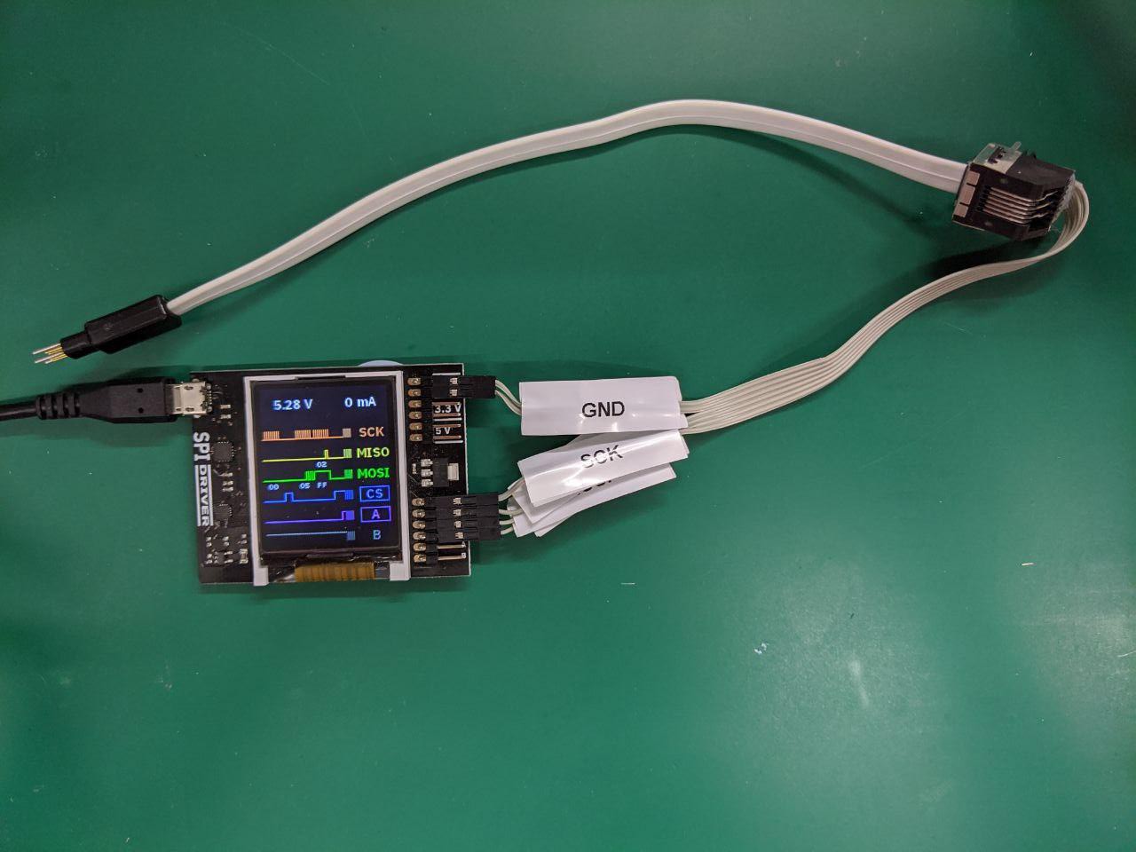
Next you will of course need to clone the repo:
git clone --recursive https://github.com/Roboy/iceboard
The cd into the iceboard folder and execute:
./software/spidriver/python/samples/TinyFPGA_BX_SPIDriver_flash.py -w software/TinyFPGA-Bootloader/boards/TinyFPGA_BX/fw.bin
The script checks for a match of the flash JEDEC id, so it will just idle until you connect the board. In order to connect the board you need to press and hold the reset button. We use a clamp to do that more comfortably but you can also just press it while flashing.
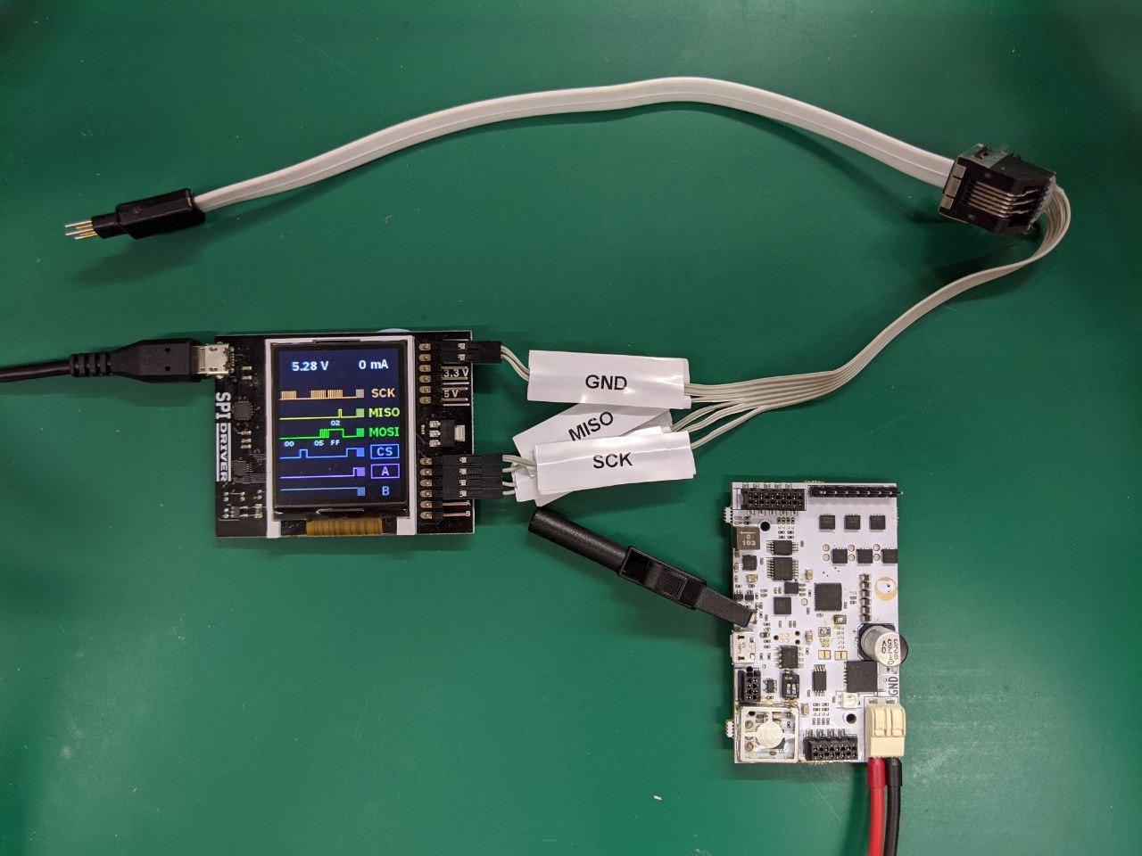
Then with the reset button pressed connect the tag-connect cable next to the flash on the board and connect your micro USB cable.
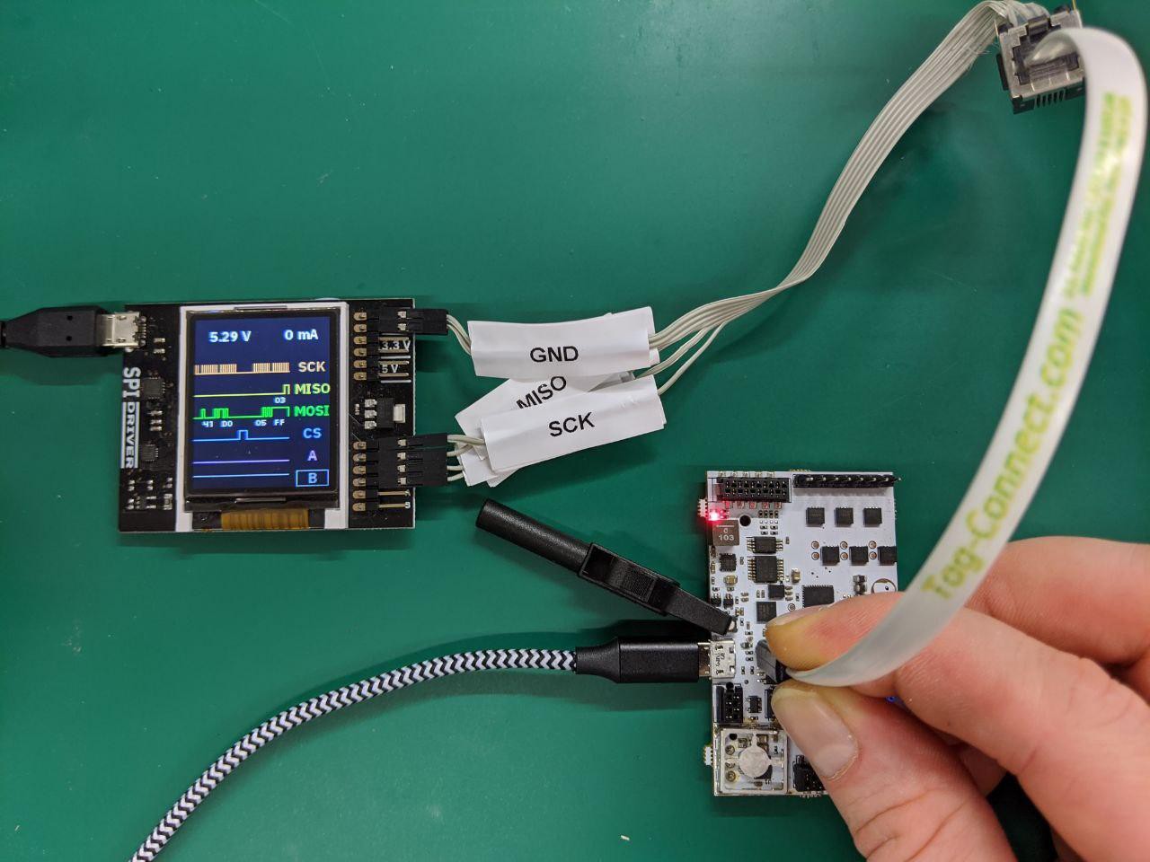
Your terminal should print something like this:
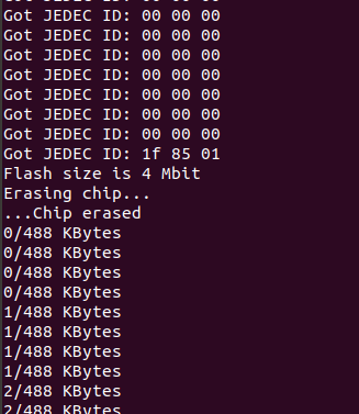
And you should see the bootloader being written into the flash in around 30 seconds. When this has finished you can release the reset button. The bootloader image should be immediately loaded and you should see the red user led pulsing every second.
If you connected the micro USB cable to your pc you should see something like this when you run dmesg:

Which shows the fpga serial2spi flash bridge that Luke Valenty implemented. We used his bootloader.v and augmented it with our gate pins being driven low. This is crucial because we are using the independent mode of the drv8323 chip giving us full control over the mosfet gates and we have to make sure all gates are deactivated as soon as possible when we power the board on.
Next we need to write the security pages of our fresh SPI flash. This is necessary to make the flash writeable with tinyprog, the python programmer of the Tinyfpga-BX board. The security pages need to contain meta-data, specifically the following:
{"boardmeta":{"name":"TinyFPGA BX","fpga":"ice40lp8k-cm81","hver":"1.0.0","uuid":"c47268cd-32d9-402f-8900-e5d10262dad2"}}
{"bootmeta":{"bootloader":"TinyFPGA USB Bootloader","bver":"1.0.1","update":"https://tinyfpga.com/update/tinyfpga-bx","addrmap":{"bootloader":"0x000a0-0x28000","userimage":"0x28000-0x50000","userdata":"0x50000-0x100000"}}}
To do this first you need to make sure you have the newest tinyprog version:
tinyprog 1.0.24.dev114+g97f6353 (tinyprog-1.0.23-114-g97f6353)
If you don't then go to software/TinyFPGA-Bootloader/programmer and run:
sudo python setup.py install
Once you have the correct tinyprog version installed you can write the security pages by executing the following commands:
tinyprog --security software/TinyFPGA-Bootloader/programmer/tinyprog/page0.bin -a 1
tinyprog --security software/TinyFPGA-Bootloader/programmer/tinyprog/page1.bin -a 2


To verify the meta data was written correctly you can try reading it with tinyprog:
tinyprog -m
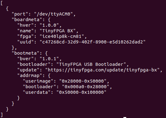
Now the board is compatible with tinyprog and we can use it to flash our user program at ease. If you have a new iceboard we recommend you install our testPins image first by running the following command:
tinyprog -p software/testPins/template_Implmnt/sbt/outputs/bitmap/TinyFPGA_B_bitmap.bin
You should see something like this:

The testPins image checks all relevant fpga pins for short circuits and the neopixel will turn red if something is wrong. If everything seems fine, the neopixel will turn green. In the following video I shorten the hall sensor pins to ground using a jumper cable which is indicated immediately by the neopixel turning red:
If the neopixel is red the full functionality of the iceboard cannot be expected and most likely the fpga is not soldered correctly.
Now, at last we can load the real deal, the motor control image:
tinyprog -p software/motorBoard_v0.1/template_Implmnt/sbt/outputs/bitmap/TinyFPGA_B_bitmap.binBTW: if you cannot load...
Read more »It's been a while since the last post, but work has continued. In December 2019 we ordered a big batch of rev 0.7 from pcbway. It was a bit of a blind shot, because we were under pressure finishing Roboy 3.0 for the Mobile World Congress in Barcelona end of February 2020. The Congress was canceled because of the Corona virus, but the motorboards turned out surprisingly bug free ;).
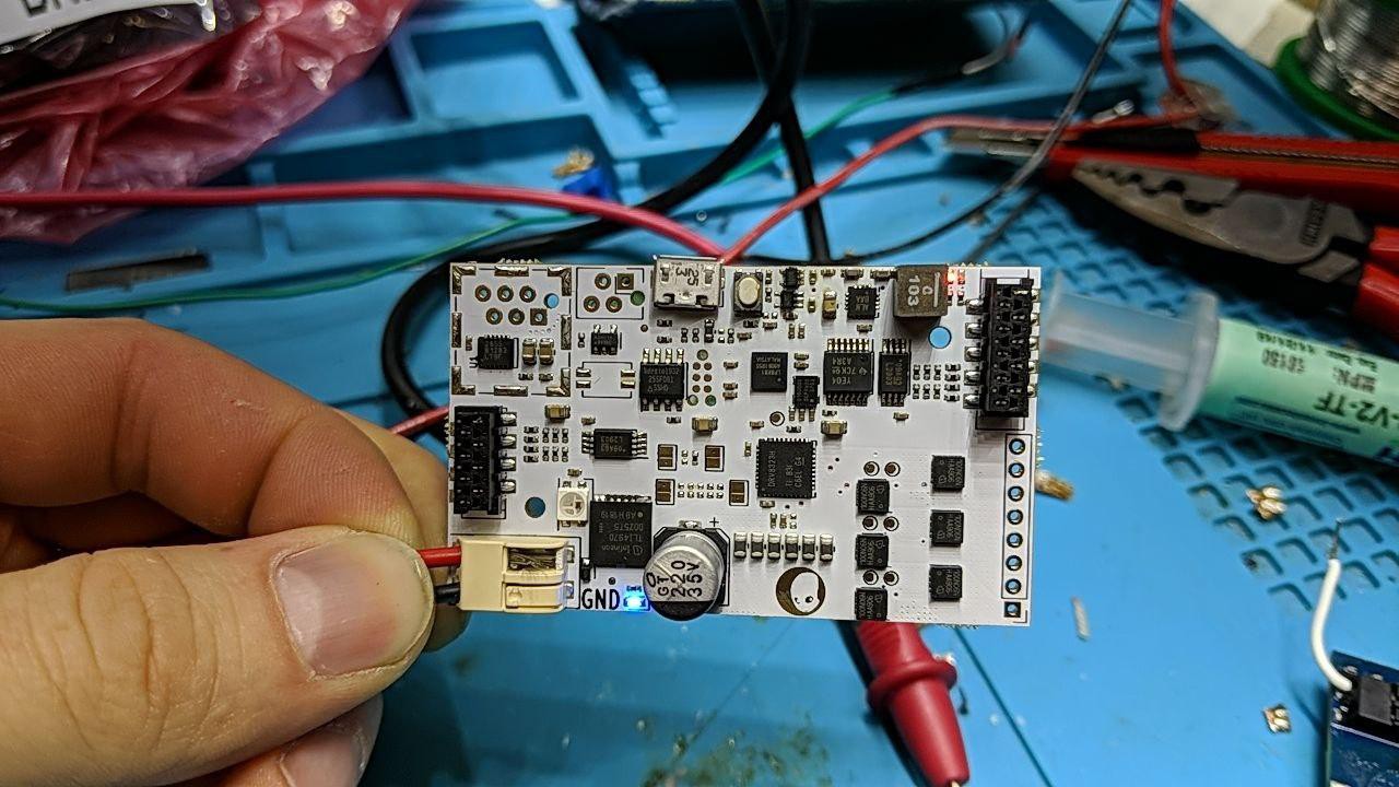
Except of course that pcbway miss-placed 94 out of 100 fpgas, which rendered most of the boards unusable. The BGA-81 footprint of the iCE40 fpga is tricky. The tiniest deviation from its target position causes short circuits underneath the fpga. The top two rows seemed functional at that time.
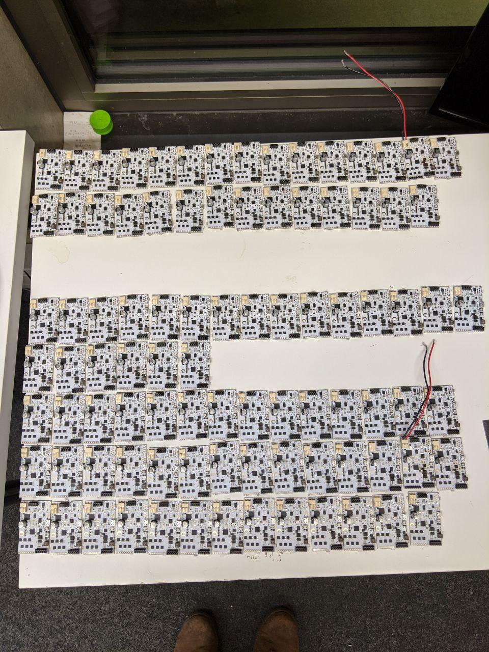
As it turned out, out of 100 boards only 6 were fully functional. Of course we complained about this to pcbway and we are shipping the defective boards back to them this week so they can resolder the fpga. I really hope they are using their x-ray this time.
Well, they are using their x-ray and the symptoms can be clearly back-traced. Pretty amazing to have x-ray.
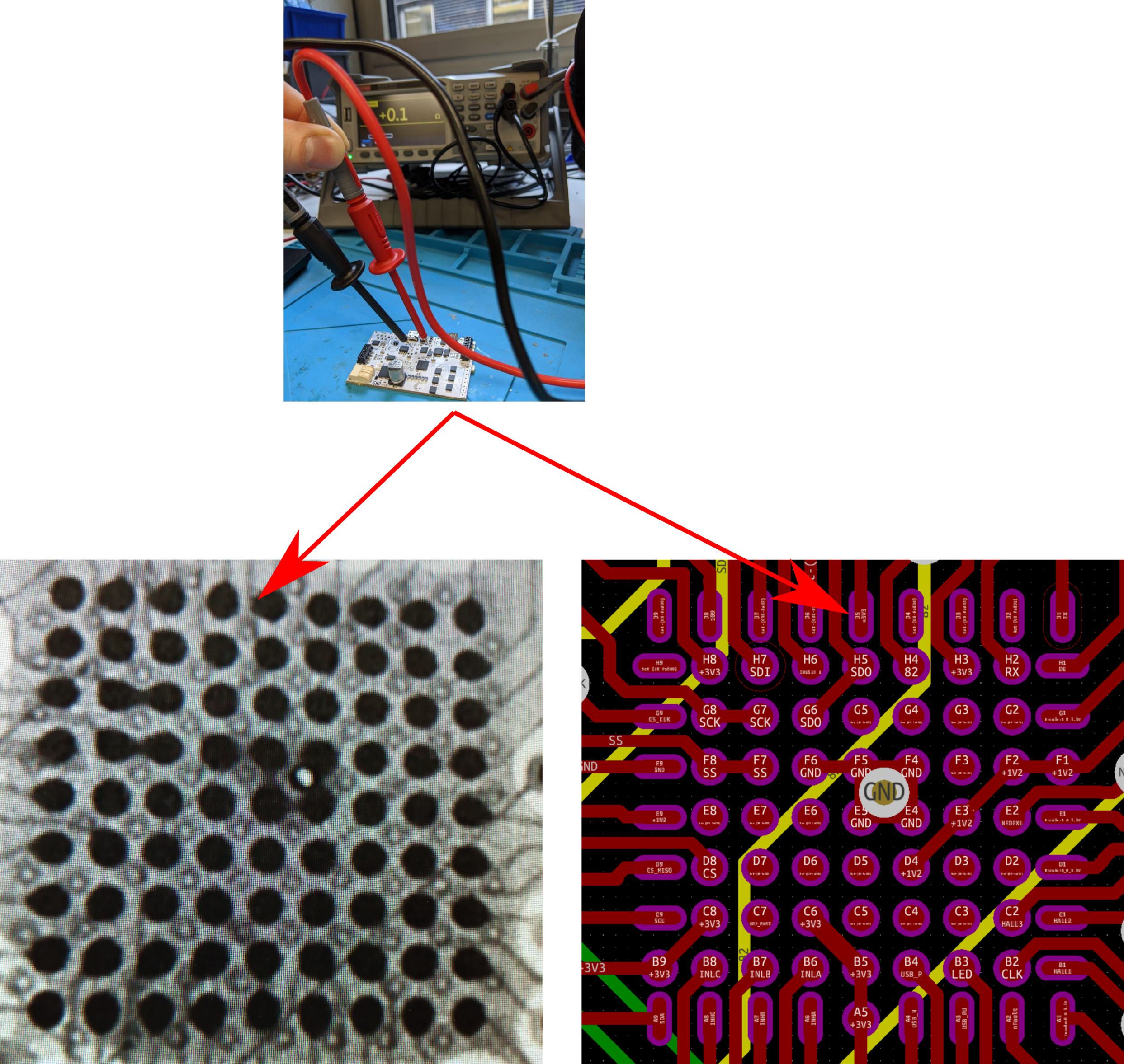
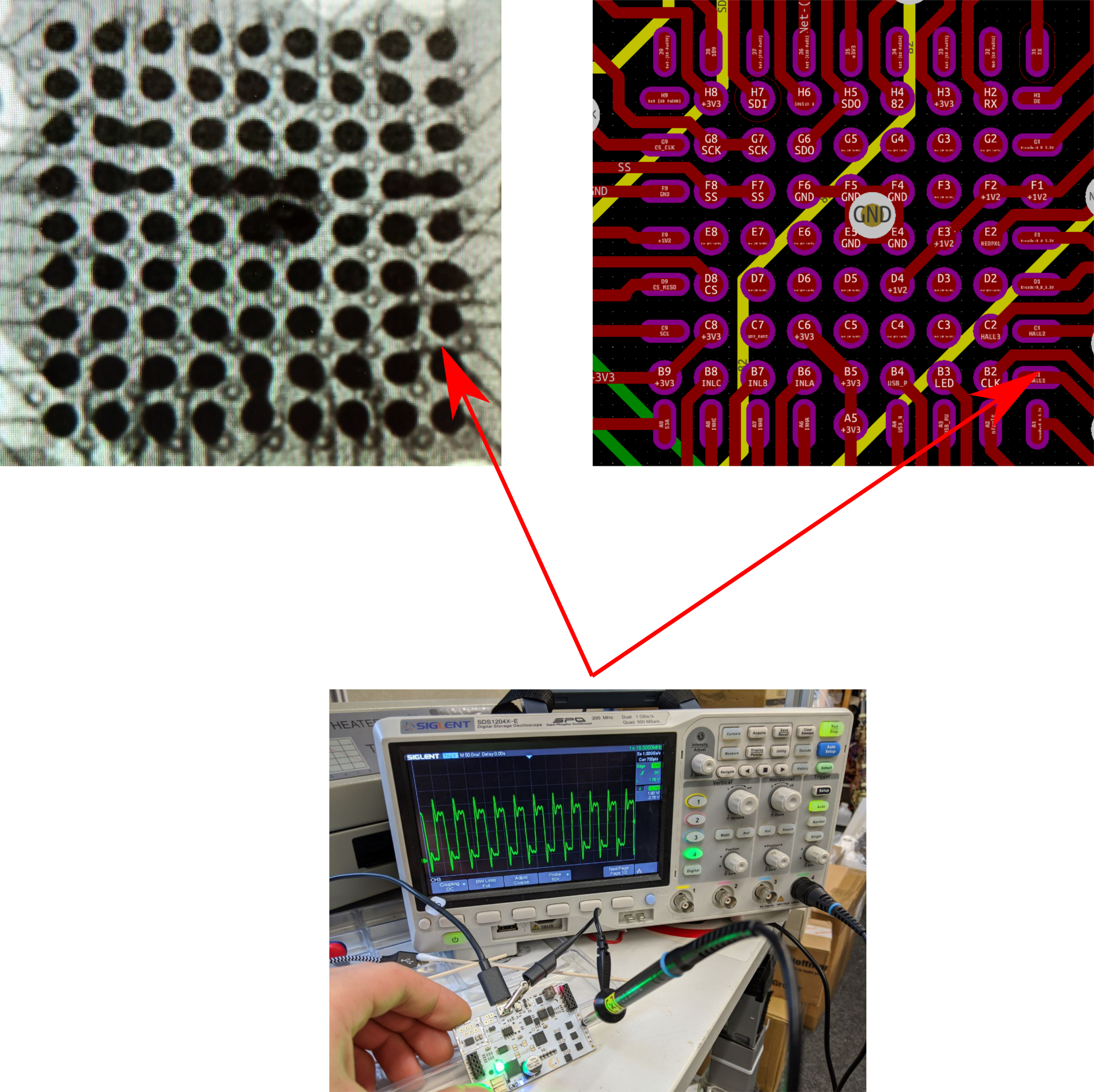
The x-rays unveil two of the most frequent defects. The first one is a short between SDO and 3.3V, which prevents the flash to be programmed. This was the case for over half of the boards. The second defect shows a short between the CLK and hall sensor pin. Both defects result from imprecise placement of the fpga too far left and too far up, respectively. So there is still hope for the bad batch to be fixed...let's see
UPDATE June 2020:
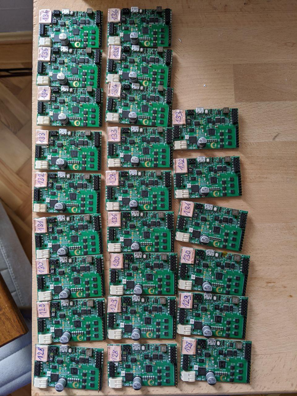
So as it turned out, there was a bug in my kicad design. Specifically when exporting to gerber, the default solder mask clearance caused the solder mask to be completely open for the ice40 fpga, which in turn made it close to impossible to solder it correctly without short-circuits. After months of debugging and discussing back and forth with pcbway, they finally agreed to redo the whole batch. The argument was that their pre-production checks should have spotted this bug. We had to pay for the manufacture of a new set of PCBs (around 600$), but they would harvest as many components as possible from the faulty boards. So finally they are in production and we can't wait to get them. In fact we inquired more manufacturers and this was very surprising to see, how expensive actually PCBway was. In Shenzhen there are literally hundreds of PCB manufacturers and it seems especially for PCB assembly it's really worth contacting as many of them as possible. We ordered a smaller batch of the v0.8 iceboards and they work out of the box. Here you can see the set to be used in roboy3:
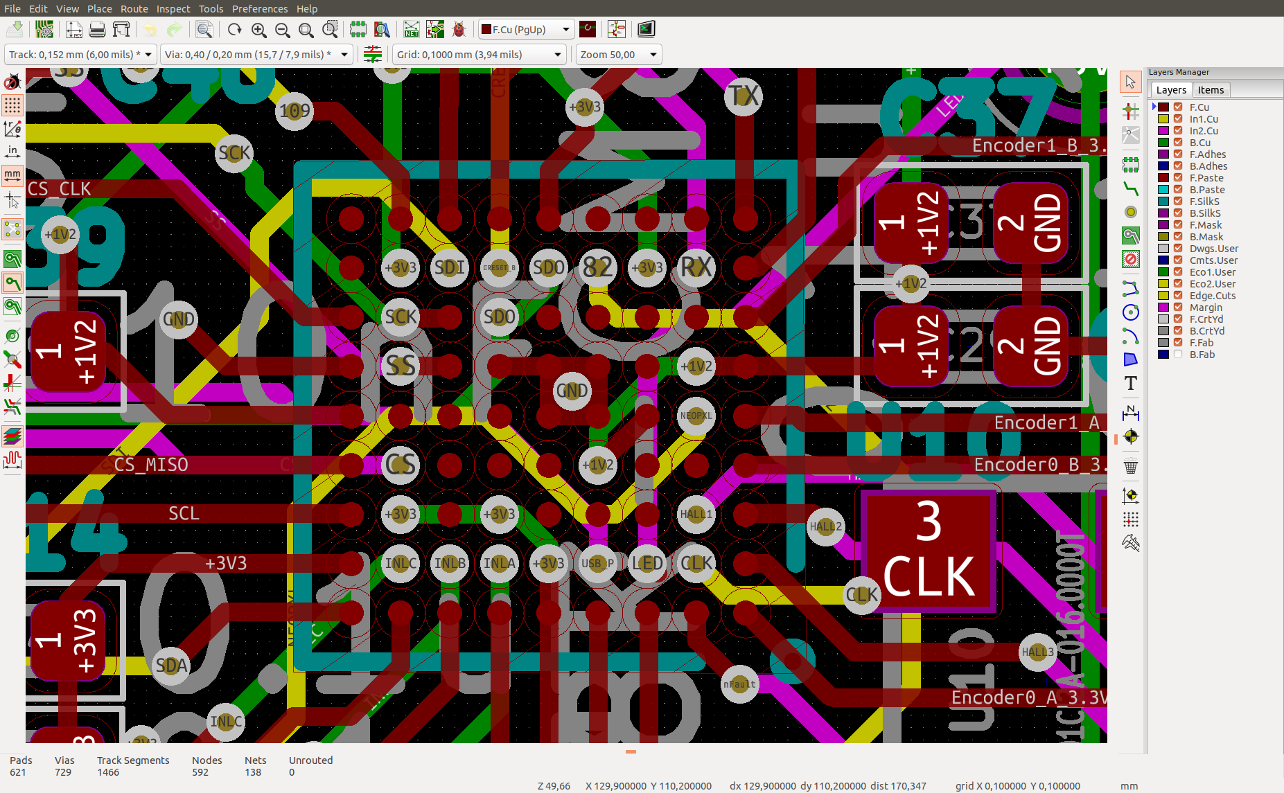
In this version I cleaned up the routing a lot, used the recommended footprint for the ice40 BGA and followed the routing design guide from lattice instead of blindly using the footprint that was used for the tinyfpga. The tinyfpga board used a footprint that was somewhat cheated into low-cost production. The footprint tries to use the outer perimeter pins of the fpga as much as possible. And the outer pads are elongated, to allow inner pads to be routed between them outwards. In this way, you can make a two-layer board, such as the tinyfpga, and route as many gpios as possible (i think it's 24 for the tinyfpga). However, if you need more pins, you should follow the design guide from lattice. They recommend four layers and blind vias. Blindvias especially can increase the PCB cost a lot, so I tried avoiding them. And as it turned out, it was possible to route all my pins using through-hole vias on our four-layer board.
So at Roboys we have been using custom motorboards from the very beginning. The problem with those has always been the communication. We have a lot of motors to control in our humanoid. The influence of EMI is huge and SPI at high frequencies was a bad choice. The past is the past, and we need to move on. For our new motorboards we wanted something more reliable but also simple to connect. The simplest bi-directional communication setup is probably UART. You may think, wait but UART sucks in terms of baudrate. Well you are correct in the realms of micro controllers. If you take fpgas however, you are free to crank up the communication speed to very high frequencies. The only limiting factor is the wiring between your nodes. When it comes to EMI your best options are:
We decided on the LTC2855 from Linear Technology, because of its max throughput (20Mb/s) and the price. This chip integrates a driver and a receiver. It translates any outgoing signals to differential signals and any incoming differential signals are filtered to a single wire. Now, on long wires and high frequencies, you must often deal with unwanted echos of your signals from unterminated wire ends. This will pollute your transmission and you should always add termination resistors to compensate for this. The LTC2855 can add these resistors for you internally, all you need to do is pull one of its pins high for this.
The following illustrates all components of rev0.5:
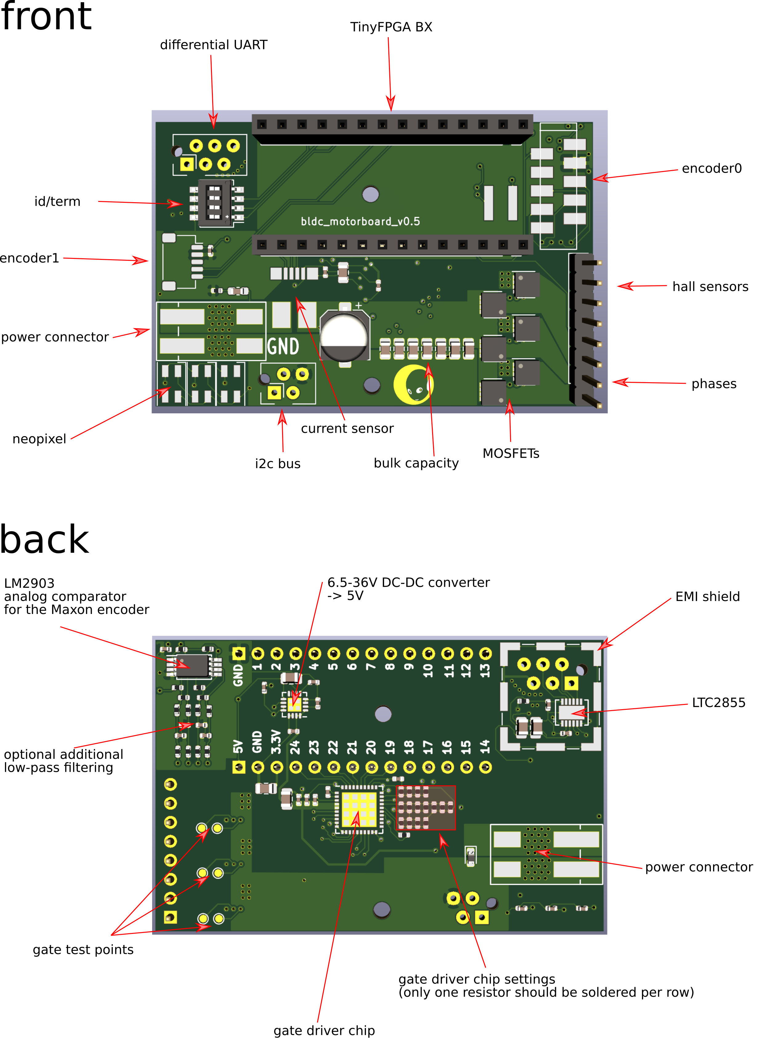
For the UART communication we decided to write our own protocol, because it's fun. So here it is (oh BTW, this is totally preliminary and very likely to change in the future):

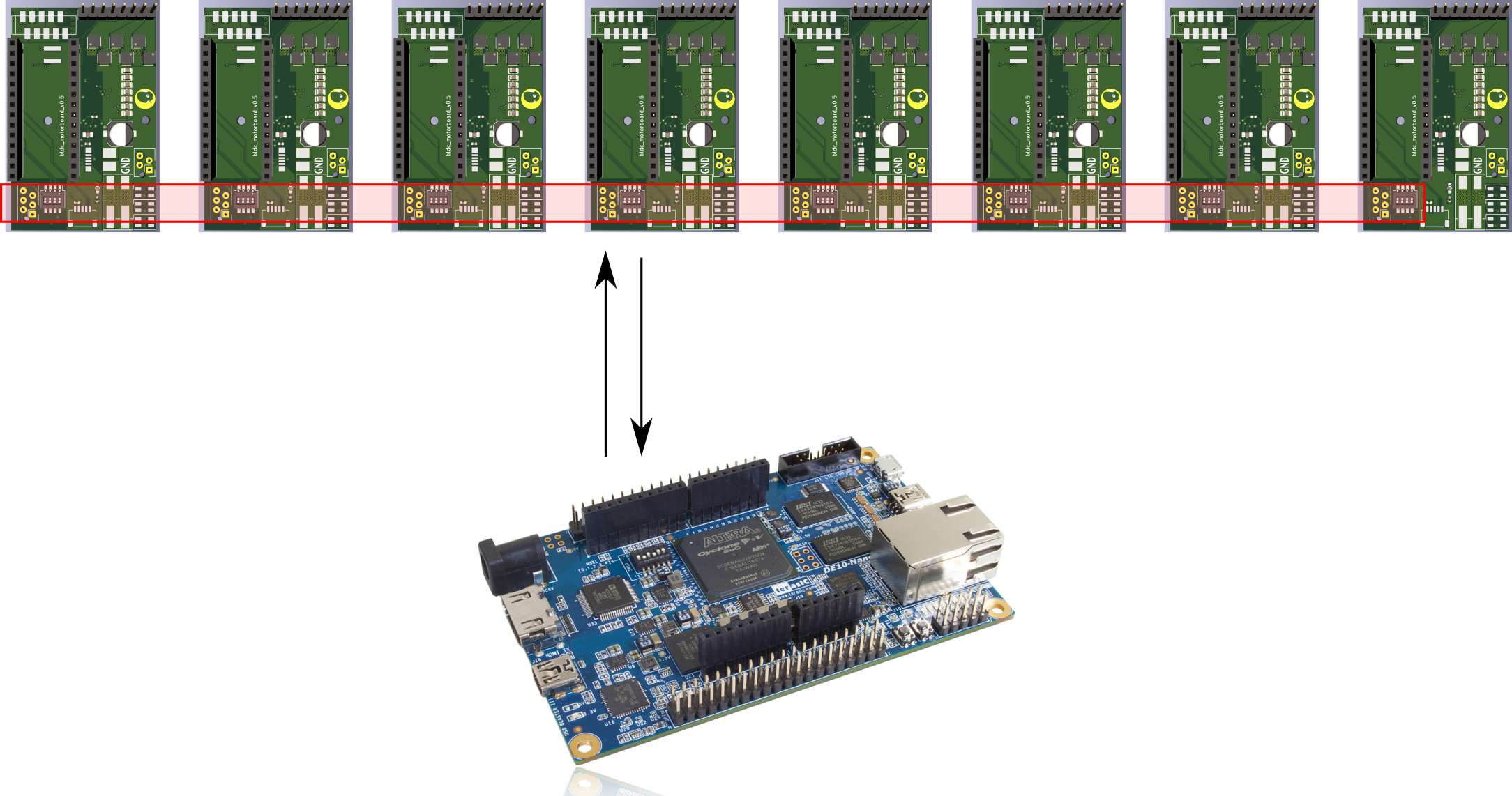
We call this the iCEbus (you get it?)
So the central node is our beloved de10-nano-soc, which integrates a dual arm core with 100k LEs FPGA. It's a dev-board from altera at about 110euro. We designed a shield for it featuring 8 LTC2855 to communicate with up to 8 motorboards per iCEbus:
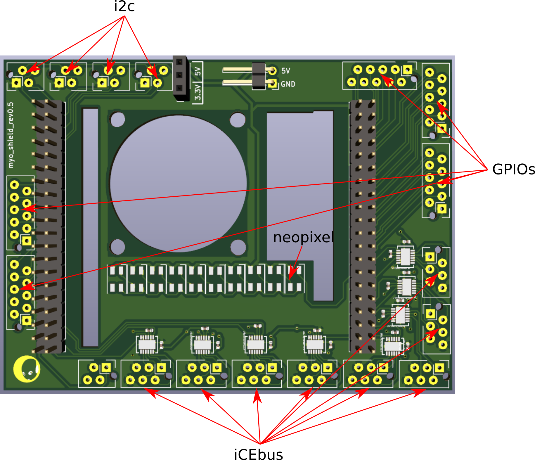
So now I would like to talk a bit more about the iCEbus protocol. It works by a header mechanism in combination with a CRC16 checksum. All motorboards listen on the data transmitted from the de10. Each one shifts in bytes received with their UART modules (adapted from opencores). If a certain header is detected, the following data is received and after having received a certain amount of bytes (depending what header was received), the CRC16 checksum over the received data is evaluated and compared to the target CRC16 checksum (transmitted by the de10). If these sums match, and only then, the command will be processed. So far we implemented four message types:
So the first two messages obviously control the setpoint and control mode of each motorboard. The third message requests a status update from the specified motorboard and the status response is the respective answer from the motorboard, obviously.
We were able to crank up the communication speed to 2MHz without any problems. This unlocks communication with each motorboard on an iCEbus with 500Hz (our target is 2kHz, but since ROS1 is not really able to handle more than 500Hz, we settled for the 2MHz for now). As I said, this protocol is very priliminary and is very likely to be augmented by different fields and messages in the future.
Control of the overall system is established via ROS. The de10 runs ubuntu 16.04 and exposes full control via custom ROS messages. These are processed in the arm...
Read more »The PCB has arrived and assembly by hand took less than an hour. It consists of a DRV8323HRTA mosfet driver from texas instruments. Six mosfets for controlling three phases and three TLI4970 current sensors from Infineon on each phase. The rest of the components is bulk capacity and connectors to the TinyFPGA and sensors.
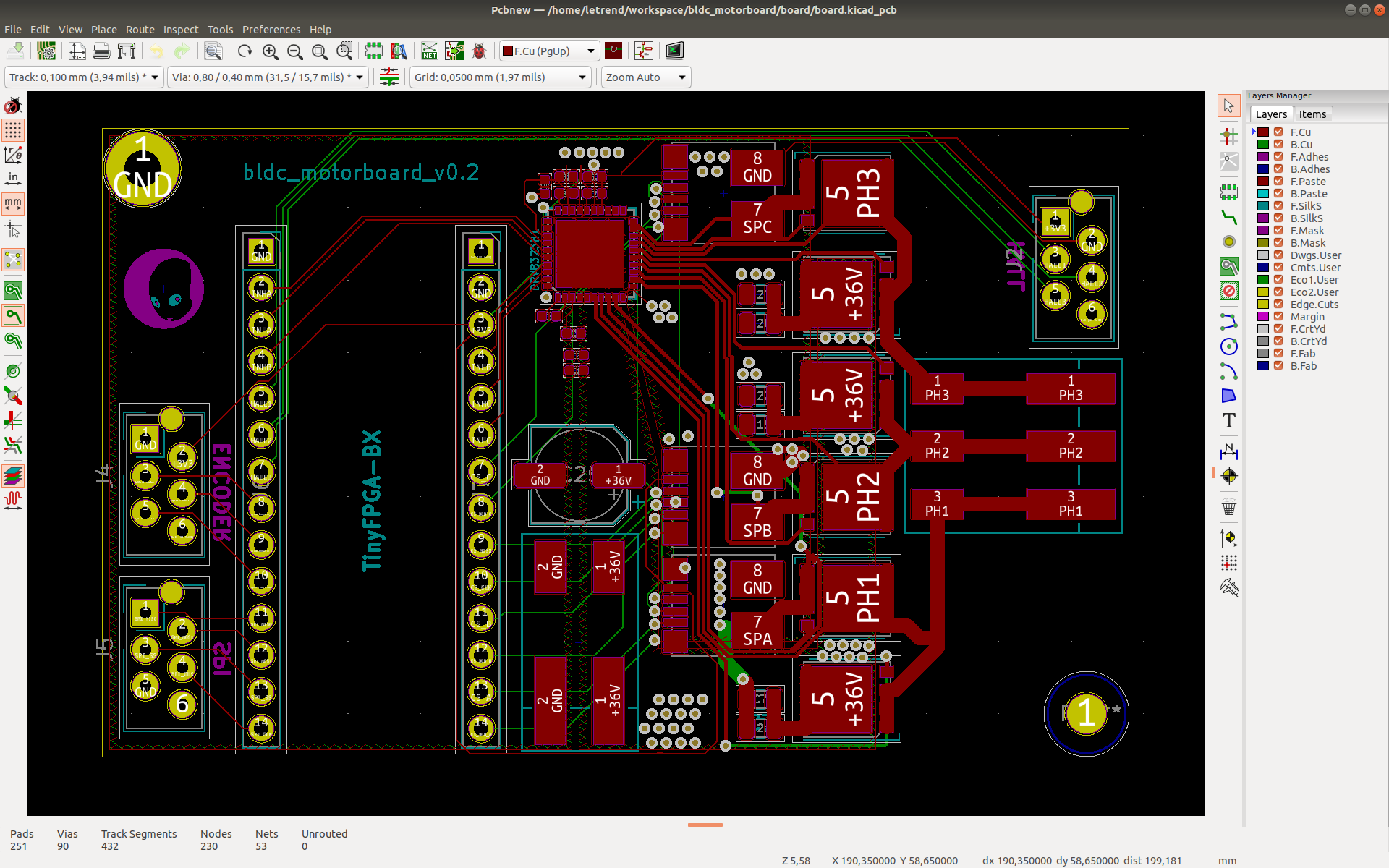
I build a small test bed keeping all components in place and labeling all cables for sanity reasons. I used a bldc motor from Maxon which has hall sensors integrated and an optical encoder measuring the motor axis rotation. The motor is fixed to the ground plane with a 3D-printed holder. The motor winch has a 4x1mm diametral magnet attached to it and an A1335 angle sensor from Allegro is used to measure the absolute winch rotation. For testing i used a MKR4000 vidor. This board features a samd microcontroller a cyclone10 fpga and even has a nina wifi module. One can code in quartus for the fpga and because the samd processor shares all its IOs with the fpga you can easily control the fpga via SPI. I use the arduino IDE for high level coding.
The verilog code for controlling the bldc motor is surprisingly simple:
assign bMKR_D[5:0] = PHASES;
reg [5:0] PHASES;
reg [9:0] pwm_delay;
reg signed [31:0] pwm;

always @(posedge wCLK24) begin: BLDC_COMMUTATION
    if( pwm>=0 && pwm_delay>(1023-pwm))begin
        if(bMKR_A[4] && ~bMKR_A[5] && bMKR_A[6]) begin
            PHASES <= 6'b100100;
        end
        if(bMKR_A[4] && ~bMKR_A[5] && ~bMKR_A[6])begin
            PHASES <= 6'b100001;
        end
        if(bMKR_A[4] && bMKR_A[5] && ~bMKR_A[6]) begin
            PHASES <= 6'b001001;
        end
        if(~bMKR_A[4] && bMKR_A[5] && ~bMKR_A[6])begin
            PHASES <= 6'b011000;
        end
        if(~bMKR_A[4] && bMKR_A[5] && bMKR_A[6]) begin
            PHASES <= 6'b010010;
        end
        if(~bMKR_A[4] && ~bMKR_A[5] && bMKR_A[6])begin
            PHASES <= 6'b000110;
        end
    end else if ( pwm<0 && pwm_delay>(1023+pwm)) begin
        if(bMKR_A[4] && ~bMKR_A[5] && bMKR_A[6]) begin
            PHASES <= 6'b011000;
        end
        if(bMKR_A[4] && ~bMKR_A[5] && ~bMKR_A[6])begin
            PHASES <= 6'b010010;
        end
        if(bMKR_A[4] && bMKR_A[5] && ~bMKR_A[6]) begin
            PHASES <= 6'b000110;
        end
        if(~bMKR_A[4] && bMKR_A[5] && ~bMKR_A[6])begin
            PHASES <= 6'b100100;
        end
        if(~bMKR_A[4] && bMKR_A[5] && bMKR_A[6]) begin
            PHASES <= 6'b100001;
        end
        if(~bMKR_A[4] && ~bMKR_A[5] && bMKR_A[6])begin
            PHASES <= 6'b001001;
        end
    end else begin
        PHASES <= 0;
    end
    pwm_delay <= pwm_delay+1;
end
The phases commute depending on the hall sensor input.
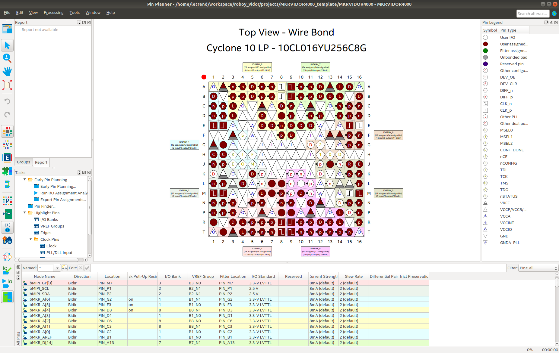
Make sure to activate a weak pull up resistor in the pin planner in quartus:
I used a poti connected to an adc pin of the vidor for setting the pwm value. There are three more sensors connected in this setup:
- optical encoder
- absolute angle sensor on the winch ( pcb / code ) connected to samd via i2c
- temperature sensor ( MLX90640 ) connected to samd via i2c
For the optical encoder I milled a simple pcb for connecting the differential signals to a chip that translates them to A/B signals. The encoder works on 5V so I put a level shifter before going to the fpga. Opencores has several quadrature decoder modules, I picked this one.
Next steps are to validate the quadrature encoder readings using the A1335 angle sensor on the winch. I want to make 100% sure I'm not missing any ticks even on highest speed.
Create an account to leave a comment. Already have an account? Log In.
Become a member to follow this project and never miss any updates

 Christoph Tack
 Simone Tolomei
 ridonkulus