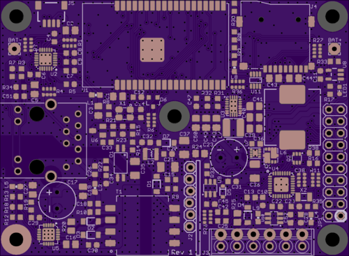
The PCB layout is done!
This was a hard one. In hindsight, it might have been better to go to a 4-layer board to get it done faster. But now it's done, I'm happy with the result and I think it will work well. To get all power and signal traces where they need to go all over the board, I needed to have extensive routing on both layers, so there isn't much left of a ground plane on the bottom layer. But with plenty of judicious via stitching between ground on the top and bottom layers, I think it's still a solid enough ground plane overall.

The PoE section on the bottom left is very similar to that found on the #wESP32. This time I'm using a smaller flyback transformer and smaller diode on the secondary side because we only need about 6W here, not 13 W as on the wESP32. The Ethernet PHY has moved to above the Ethernet jack. This means it's closer to the jack than on the wESP32 so performance should be as good or better.
We moved from an ESP32-WROOM-32 to a ESP32-WROVER-I module to take advantage of PSRAM for larger projects and have plenty of space for MicroPython. The positioning of the module may look bad for antenna performance, but since we use the -I version with U.FL connector and an external antenna, the on-board antenna is not used, and the module's position is fine.
Programming and serial console is provided by a wESP32-Prog submodule as on the wESP32, the footprint for this option (J2) is located central on the PCB along the bottom edge as on the wESP32.
Most of the new stuff is on the right side of the PCB. On top is a micro SD card slot, wired for 1-bit access from the ESP32. 1-bit is not the fastest but it's a compromise to preserve enough ESP32 pins for GPIO connections to external circuitry. I wanted to have at least enough pins available for simultaneous use of I2C (2 pins) and SPI (4 pins), and with the pins taken up by the Ethernet RMII bus (8 pins) and the PSRAM (2 pins), and the unfortunate number of input-only pins on the ESP32 (4 pins), 1-bit SD access was as good as we were going to get.
Central on the board is the buck-boost converter that generates the 3.3 V system power from the battery voltage, which can range from 1.71 V to 3.6 V (minimum LTO to maximum LiFePO4 voltage). The converter should be able to provide at least 1 A even at the lowest input voltage. The central location worked out well to use a star topology for system power distribution.
To the right and below this is the microcontroller based charging system. This was the hardest part to layout because the various current loops need to stay as small as possible to reduce EMI and maintain high performance. I went with the NCP81151 based gate driver to minimize cost and take advantage of the built-in zero cross detection and synchronous rectification for maximum efficiency. This came at the cost of more components for regulation and level shifting, so it was a very tight squeeze to pack it all in. I had to use resistor, capacitor and transistor arrays to make it work.
External connections are clustered on the bottom right. The reason for this is that I wanted to keep the top edge of the PCB clear of through-hole components so it is possible to install an optional on-board 18650 battery holder there on the bottom of the PCB between the BAT+ and BAT- pads. Since the battery holder makes the mounting holes along the top unreachable, a central mounting hole was added as well. The on-board battery should be a good option for development and bench-top use, but I expect that most production installations will use an external battery connected to the screw terminal connector along the bottom, along with DC/solar power input, if that is used.
The GPIO header needs to be in the bottom right as well for the same reason, to not interfere with the optional on-board 18650 battery. This made the layout harder because a lot of traces needed to be routed from the header to the ESP32 module.
Initially I was trying to keep the GPIO header pinout as similar to the wESP32 pinout as possible, but I gave up on that. The product is very different and with the reduced number of ESP32 signals available, plus extra power buses, it was going to turn out very different anyway. The header is going to have 4 power buses (V+ external power in/out, battery voltage, switched battery voltage and 3.3 V system power), 10 ESP32 GPIO signals (on the 3.3 V regulated power domain) and 3 charge/system controller GPIO signals (on the 1.71 V - 3.6 V power domain).
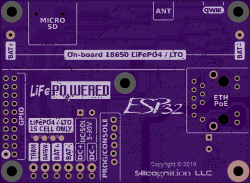
I decided to add a convenience for users this time by including a legend on the bottom silkscreen of the PCB:

This should help make it clear where various parts need to be connected. I had initially hoped to also provide a GPIO legend but there just isn't enough room.
As you might notice on the legend in the top right, one last-minute addition is a Sparkfun Qwiic connector! Since the board has a dedicated 3.3 V level I2C bus already for communication with the charge/system controller, it made sense to add this. Adding this convenient small connector opens a world of possibilities to be able to use this board for real-world applications without having to make a daughter board at all!
Next step: prototype boards. I have contacted KingTop Technology to see how much it costs to have a small number of prototype boards produced. If it's reasonable, this may be the fastest route to prototypes, otherwise I will have to build them myself.
 Patrick Van Oosterwijck
Discussions
Become a Hackaday.io Member
Create an account to leave a comment. Already have an account? Log In.