For the past few days, I've been working on developing a simple test program for my CTC. The goal of the software is to print "Timer start", wait 1 second, and print "Timer done". The timer runs off of the system clock (6MHz) so that it can be divided into exactly 6Hz. This is done by setting up a timer with a 16x prescaler and 250 time constant, the zero output of which is fed into a counter which counts down 250 events. Each time the counter hits 0, it throws an interrupt, which the CPU then handles using an interrupt routine. Each time the interrupt routine is called, the CPU adds 1 to a memory cell. If the cell is equal to 6, the timer is finished and "timer done" is printed, ending the program. The math ends up looking like this:
(((6000000/16)/250)/250)/6 = 1Hz
Therefore, the timer lasts for exactly 1 second. Of course, you can change the duration of the timer by editing the value in the RAM cell that the program checks for. You can find the code here.
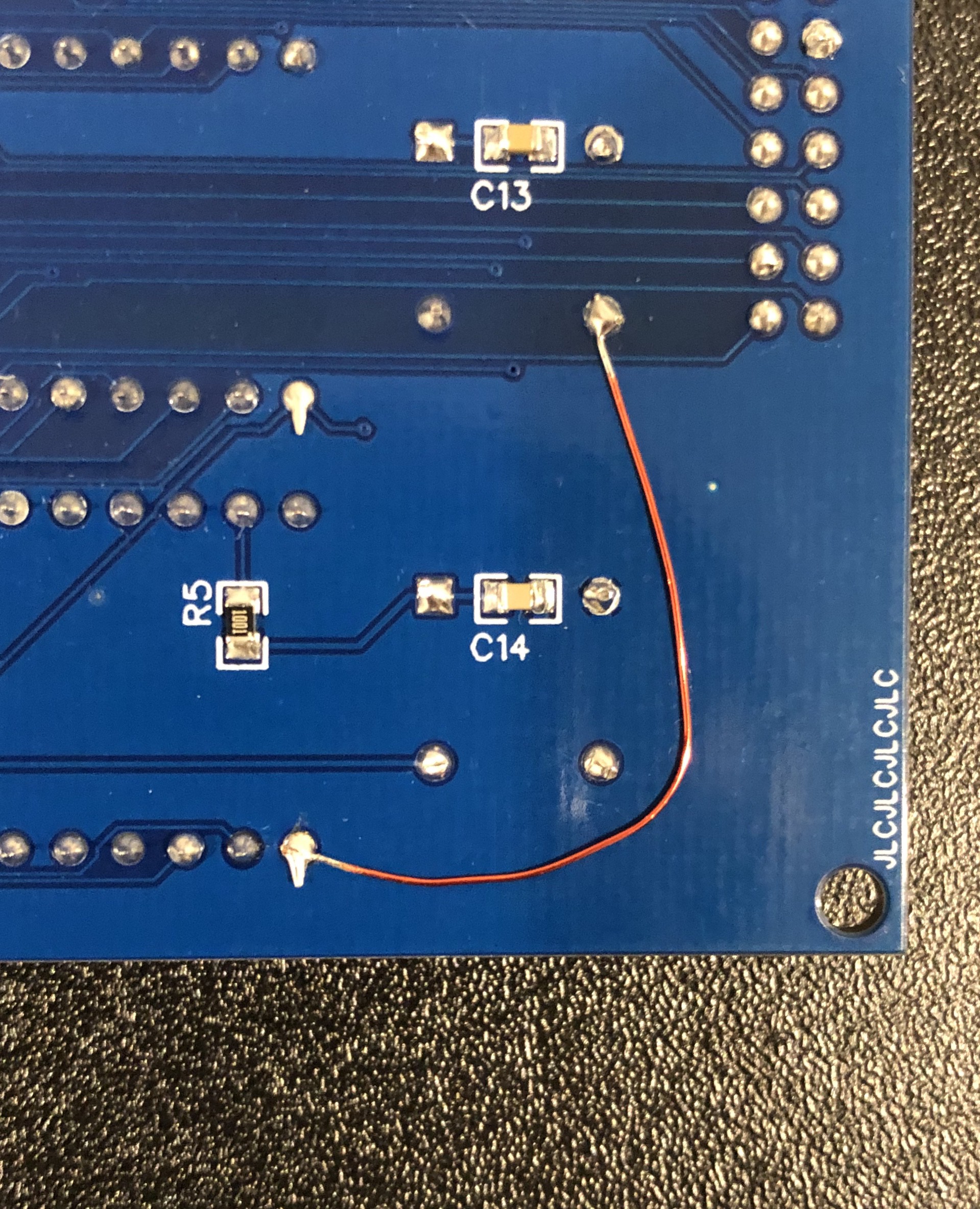
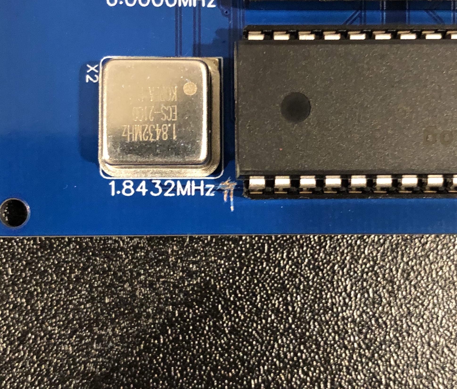
As usual, there were some hiccups along the way. As I was testing the program, I realized that the CPU was never running its interrupt routine, which meant that either the routine was programmed incorrectly or that the CPU was never receiving a pulse on its INT pin. The problem happened to be the latter of the two, and so I looked over my CTC programming to see if I had made any kind of mistake, which I hadn't. With software out of the way, I began to debug hardware. After analyzing my PCB schematic, I noticed that I had hooked the baud clock signal up to the CLK pin of the CTC. I had done this on purpose, as the baud clock could be easily divided into exactly 1Hz using only one timer. What I failed to realize is that this caused the CTC to be out of sync with the CPU (duh) so they couldn't communicate. Oops! With an X-Acto knife and a bit of enameled copper wire, I was able to hook the main clock signal up to the CTC and disconnect the baud clock.


This wiring issue, along with a few other issues, have been fixed in version 2.1 of my PCB. The most important of these fixes include better CMOS support (no inputs left floating), moving the ROM socket for easier access, adding a TTL serial header on the SIO channel B, GND pins on the PIO headers along with a common cathode pin for the flyback diodes on channel B, and some general layout changes.
I should have some new PCBs within a few weeks and I'll update on any changes before then, as well as updating the project details section.
 Jacob Hahn
Discussions
Become a Hackaday.io Member
Create an account to leave a comment. Already have an account? Log In.