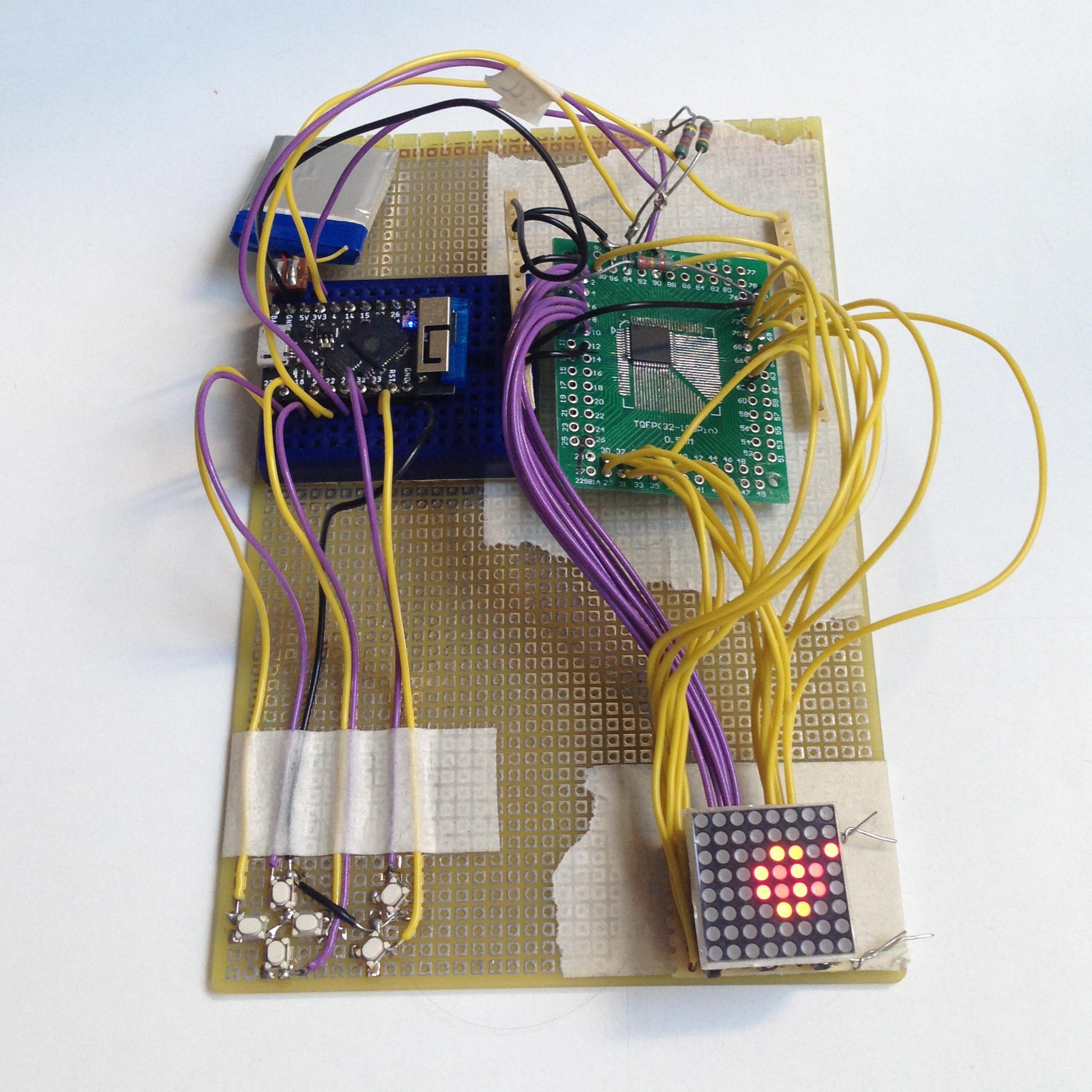
With the prototype circuit working, it was time for the interesting part: PCB design! I planned to use EAGLE for that, I had used it before and had gotten somewhat familiar with its quirky user interface. I had version 7.5 installed, which was from before the acquisition by Autodesk, and didn’t bother checking if they had managed to ruin it yet in newer versions. Someday I should, but then I also resolved that for some future project I’m going to try KiCad and see if it’s any more or less capable and compatible with my brain.
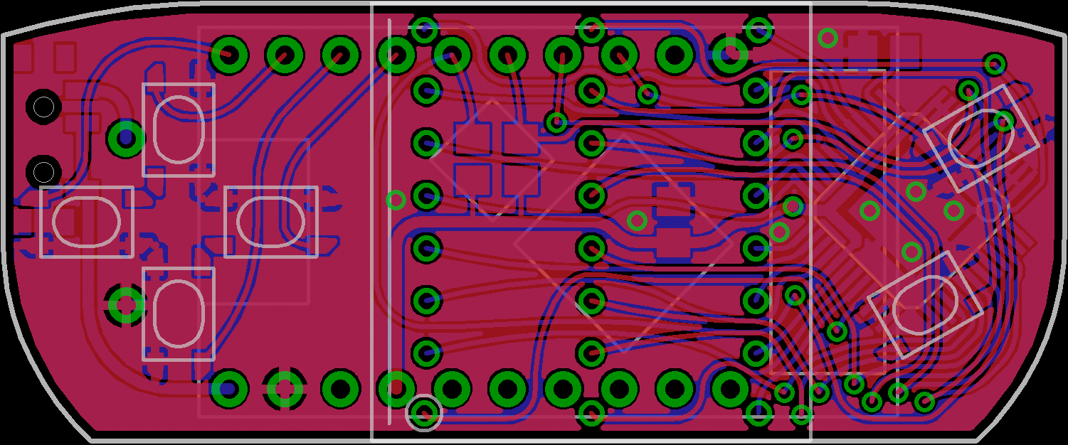
The main challenge in the basic layout was posed by the fact that the spacing between the outer rows of pins of the LED matrix was pretty much the same as that of the TinyPICO, meaning that I couldn’t put them exactly on top of each other. I didn’t want to offset them sideways either however because that would make the board larger, and I was really trying to get it no wider than the LED matrix, 20 mm. A promising idea came in the form of @de∫hipu’s #Matrix Sanitizer, where he had rotated the two layers of pins by 90° relative to each other, which made them interlock perfectly, although with very little space left for pads. These were both on a 2.54 mm grid though, and my matrices had a 7.5 mm by 2.4 mm grid, which didn’t fit between the TinyPICO’s 2.54 mm pins at all. However, since I had found that the matrices could be crammed into a 2.54 mm grid with some force to bend the wires, what about bending just the outer 6 pins into the 2.54 mm grid and leaving all the others on the 2.4 by 7.5 mm one? That worked beautifully on the screen, and it even let me run a trace between the pads on the inside of the TinyPICO pins, which wouldn’t have been possible with all matrix pins on the 2.54 mm grid, but turned out absolutely necessary. How well it works mechanically with the actual matrix remains to be seen when the PCBs arrive.
I proceeded with placing the ISSI chip and wiring it up to the matrix, which turned out harder than expected: The pin row of the matrix closest to the chip caused a bottleneck, acting like a fence through whose gaps a lot of traces needed to go. When using 8 mil traces, I could run two of them between each pair of matrix pins on both sides, except for the outermost ones, where only one would fit because a TinyPICO pin was in the way. That gave me space for 24 traces – just barely enough for 16 matrix pins, 2 I²C lines, 2 buttons, and 2 power lines if I made those 20 mil wide. Whew!
After several iterations of nudging the ISSI chip around to get it farther away from the corner of the board so I could round off more of it, and the corresponding twiddling of traces between the matrix pads, I had a rough layout that satisfied both the design rule check and my desire to squeeze things neatly together for the tiniest board outline possible. It consisted of the usual 45°-angled traces, placed by hand somewhat irregularly because of the different grids involved. That I was not happy with, I want my traces curved, not angular, aligned to the environment, not to an arbitrary grid, neatly curving around obstacles and regularly spaced where several run in parallel.
So, a final round of prettification started. EAGLE’s tools however turned out severely inadequate for that. Maybe not surprising, because this is work that no engineer working on a commercial product would do – but I have the luxury of being a hobbyist, here to spend more time on it because I’m having fun, not less because it costs money. What to do? As always, make your own tools.
EAGLE can be extended with so-called ULPs (user language programs), and learning how to do that was an interesting experience. They are written in a C-like language that is easy to pick up using the documentation, but the system is very awkward because these programs cannot modify the internal data structures of the document, to bend or add traces as I wanted. The document tree is read-only, and the only thing the program can do to modify it is to generate a script that is executed at the end, consisting of commands that basically simulate mouse clicks and command-line entries – it can only do things that a human could do through the UI too.
This required some workarounds and awkward UIs, but in the end I succeeded in making the geometrical tools I needed for my layout prettification: ULPs that make tangents to arcs, intersect lines, tangentially extend or offset curves, interpolate with biarcs, and place wires exactly centered between two pads. I might release them in the future after they mature some more.

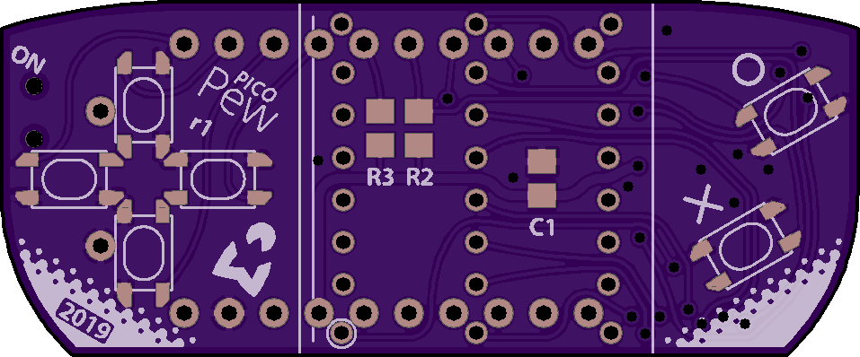
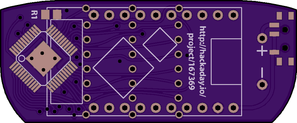
After prettifying the traces, I turned to the silkscreen. Apart from minimal component labels, I wanted logos, revision information, the URL of this project, and some decoration there. For the graphical elements, there are converters that can import SVG into EAGLE, but I seemed to remember that last time I tried that, I wasn’t quite satisfied with it, so I did it my own way: After preparing the polygons in the right way in Inkscape, converting them from SVG path syntax to EAGLE’s XML library format becomes a simple series of text search-and-replace operations.
For the text, since I consider EAGLE’s built-in vector font aesthetically beneath my dignity, I had previously done the same thing for some reusable elements like “ON” and “OFF” labels, but that approach wouldn’t scale to one-off things like the project URL. Instead, I made a library containing all ASCII characters as polygons in a nice font derived from Myriad, created in Inkscape using curve-offset and flattening operations, and many manual tweaks where those didn’t yield satisfying results. (Myriad, despite looking quite even, has a suprising variance in stroke width and is not easy to approximate with a constant stroke!) Together with a ULP that would string these glyphs together in the correct advance widths, I had a rudimentary typesetting tool for acceptably-looking text – even though again with an awkward UI: because a ULP has no access to library elements that aren’t already present in the document, it needs to import all needed glyphs first (heaping them on top of each other), and them measure and typeset them in a second call. (I could have stored the advance widths in the ULP instead of the library to avoid that, but that didn’t feel right either.)
I had chosen different GPIOs for the buttons on the PCB than in the prototype to simplify the layout, and also wired the LED matrix to the ISSI chip a bit differently, partly for the same reason. The other reason was that in the prototype, I had wired all the green column pins of the matrix to the first half of CS outputs and all the red columns to the second half, which made for an awkward layout of color values in the frame buffer. On the PCB, I had now wired the green and red columns alternately instead, which meant that the green byte and the red byte of the same pixel would now be adjacent in the frame buffer. I rewired the prototype to match that layout and adjusted the software.

That worked, and after a final double-check that the wiring of the prototype matched the PCB, as well as inspecting the Gerber files in Gerbv and printing them out in original size to check if I had gotten all the component sizes right, I was confident that the board was ready for production. I placed an order for a prototype batch at OSH Park and got these nice pictures.


Miraculously, the rewiring of the prototype had also fixed the one dead pixel – I could now turn on all the LEDs. How could that be? I was expecting that there would simply be a different dead pixel now. Apparently it wasn’t a broken memory cell after all, but how could the wiring affect a single LED? I was quite perplexed, until I remembered that at the end of the rewiring, I had removed an accidental solder bridge between two stripboard traces from the matrix base board, which I had assumed had happened during the rewiring. Apparently not, it had been there all along, and by connecting one row pin to one column pin, it shorted out one LED. Doh! I could even have detected that in software using the short detection, but for some reason it hadn’t occurred to me to try that.
This post concludes the retrospective series, we have now caught up with the current state of the project. I am waiting for the PCBs to arrive from OSH Park, which should happen in the next few days, and am eager to try out if my design works!
 Christian Walther
Discussions
Become a Hackaday.io Member
Create an account to leave a comment. Already have an account? Log In.