 smartroad
The prototype PCBs turned up this week and I have been having fun getting then working. I am still reasonably new to soldering SMT but flux is my friend! Even so, I was still having problems reprogramming the ATMEGA on my board. Turned out there was a minuscule solder jump between the SPI clock pin and the adjacent pin on the chip. Once I had that clear the chip took on the firmware with no issues.
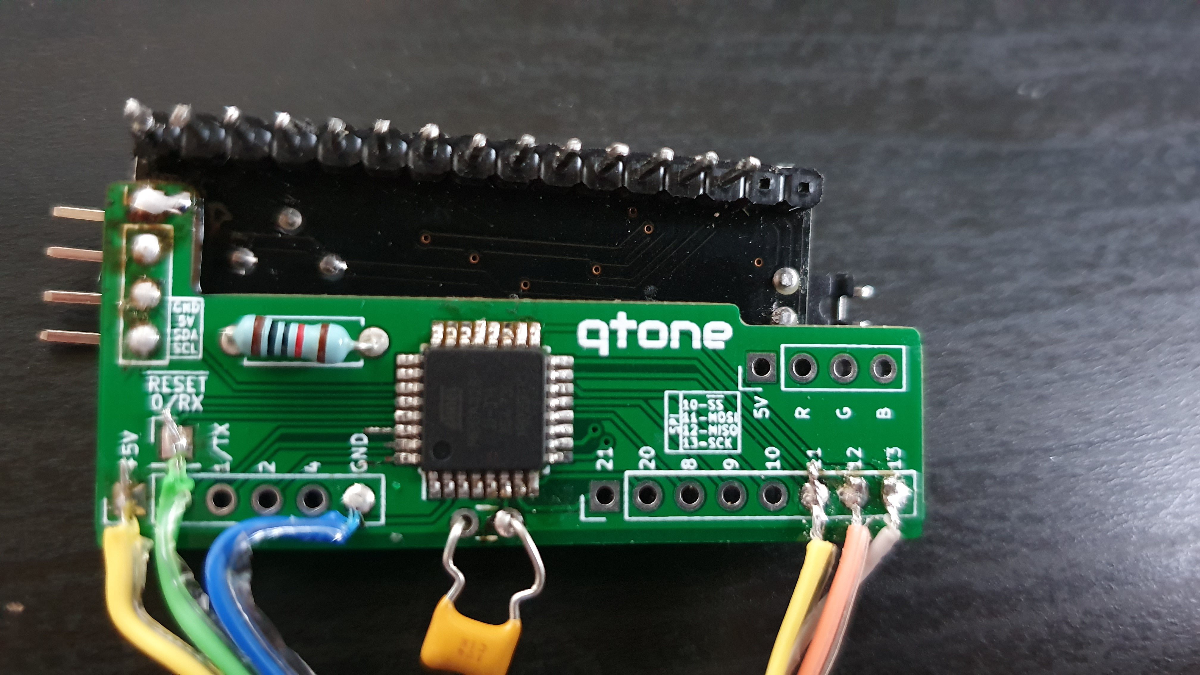

There are some changes I would like to do to the PCB. As mentioned in the image above I've had to wedge the boards apart to make the LCD backpack work. I de-soldered the connector to allow my backpack to attach, but I don't think the solder has flown back down fully. Next version I will use larger holes so the connector can stay soldered.
Also my backpack doesn't lay flat as I have used through hole parts for the resistor and capacitor. The resistor is the issue as it obviously comes through. I have two thoughts on this. The obvious is to go over to surface mount components. The second is to solder the top side so the excess legs can be cut flush.
To finish off this log; another video demo!
Discussions
Become a Hackaday.io Member
Create an account to leave a comment. Already have an account? Log In.