Today I got the datapath working ! I mounted all parts, except those that are in the address generation section, because I wanted to start small. Also, no memory is mounted yet.
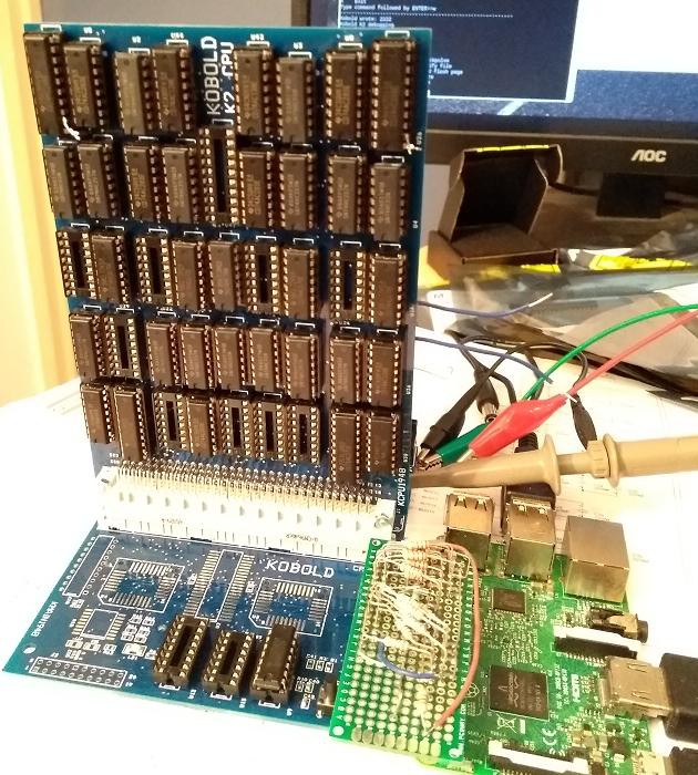
As intended, the main board connects to a Raspberry Pi. At this moment, the connection has:
- 16 databus lines
- clock_enable ENA output to Kobold (GPIO24, low to disable Kobold clock)
- clockpulse CLK output to Kobold (GPIO8, clockpulse is active high)
- chip-enable CE output to Kobold (GPIO3. If high, Kobold and memory will not drive the databus)
- EXEC signal from Kobold to RPi. Low for an exec cycle, high for a fetch cycle.
The RPi can control the Kobold, that is needed for debugging and lateron for programming the flash. It will use the ENA output to stop the clock of the Kobold. It can then use the CLK to give a single clockpulse, and watch the EXEC signal to see if Kobold expects a Fetch or Exec cycle.
In a fetch cycle, RPI must make CE high, then put an instruction on the databus, and give a clock pulse. The Kobold will place the instruction in the instruction register (U27 and U28) (with the "I" command in the Python script). The following exec cycle can be a read or write cycle. In a read cycle, the script must put data on the databus ("M" command in script) and give a clock pulse. The Kobold will think that it reads this from memory.
If the exec cycle is a write cycle, use the "W" command in the script. The RPi must make CE low, to enable the data output of the Kobold. It must also make its 16 datalines input. It can now give a clock pulse, and just before the end of the clock pulse it can read the data on its 16 datalines, and put that on screen.
The following sequence is used in the Python script to add 1234 to 4321 :
S       # stop Kobold clock
I 6400  # fetch: instruction to load a word in register D0
M 1234  # exec: provide the data that Kobold reads from memory
I 4400  # fetch: instruction to add a word to register D0
M 4321  # exec: provide the data
I 9400  # fetch: write data from register D0 to memory
W       # exec: Kobold writes result to memory, RPi catches
                 it and displays 5555
The Kobold has no addressing system yet. It is not needed for this test because the RPi handles all reads and writes, and also is agnostic of Kobold memory addresses at this moment.
I also successfully tested the NOR operation and the data registers.
It took a few days to reach this point. The HC299 has kept me busy. You could write data in it, but it always returned zeros. How difficult could it be ? Two inputs determine what happens at a clock pulse: Do Nothing, Load data, Shift Left or Shift right. Two enable inputs must both be low to put the contents on the bus.
After a day of debugging, I read the datasheet word by word. And there is was:
Both output enable (OE1 and OE2) inputs are low and S0
or S1 or both are low, the data in the register is presented
at the eight outputs.
So S0 and S1 must not both be high when you want output ! Always read your datasheets.
After that, the system suffered from unstable behaviour. Sometimes it worked, and the next minute it didn't. This was finally traced down to my start-small strategy, where the address generation chips were not yet placed. I simply overlooked that a control signal that was needed for the data system, was routed through one of the missing chips. The signal was now undriven, that explains the strange behaviour.
Discussions
Become a Hackaday.io Member
Create an account to leave a comment. Already have an account? Log In.
Gefeliciteerd!
Are you sure? yes | no
Dankjewel, Marcel !
Are you sure? yes | no
Congratulations!
Are you sure? yes | no
Thank you, Ed !
Are you sure? yes | no