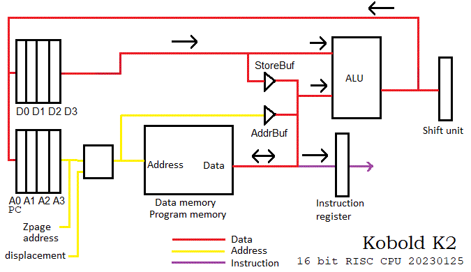
CPU BLOCK DIAGRAM
[ edit 20230125 more accurate drawings and more explanation ]
Main parts are:
- 4 data registers D0 - D3 (16 bit)
- 4 address registers A0 - A3 (20 bit)
- 16 bit ALU that can do only ADD and NOR
- shift unit that can shift one position to the right
- instruction register
- Single memory for program and data
Every instruction needs two cycles:
EXECUTE CYCLE
This will let the ALU calculate a new value and put this in the shift unit. Or it will store a data register in memory.
The inputs for the ALU are:
- a data register and a memory operand, or
- a data register and an address register
- a data register and a short 8-bit immediate
For memory operands, the address comes from an address register and displacement, or it is a zero-page address. 16 bit immediate operands can be selected by using the program counter as address register (and using a displacement).
Most of the parts in the CPU are directly controlled by bits in the instruction register, just as in the Data General NOVA whose instruction set is found HERE.
FETCH CYCLE
The contents of the shift unit is transferred to the destination register. The contents can be either shifted or unshifted. The PC (address register A0) is connected to the memory address. The next instruction is fetched from memory and is put in the instruction register.
Incrementing the PC will be discussed later.
DATA FLOW FOR MAIN INSTRUCTION TYPES
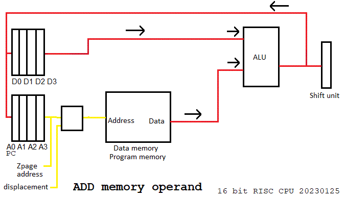
This shows how data from memory is added to a data register.
The 4-bit displacement (coming from the instruction) is added to the selected address register to form the address. (Displacements are added to bit1 - bit4 and the address register contents must be aligned). In zero page mode, the address comes from the lower byte of the instruction.
The ALU can do a ADD or NOR operation. The result of an operation goes to a data or address register. By making combinations, the following other functions can be obtained:
- MOV: The ALU can transfer the memory data to a register without change. This is done by forcing the data register output to zero and set the ALU operation to ADD.
- COM: A register can be bitwise complemented by NOR'ing it with the value #0.
- SUBTRACT: First complement one of the operands. Then do the ADD and finally ADD #1. Both ADD instructions can be done by a single ADDI (Add and increment) instruction.
- OR: Do a NOR followed by complement-register
- AND: First complement both operands, then do NOR
- JMP: The program counter is in A0, so a jump is just a MOV to A0.
Complementing a value (bitwise) is often used in this architecture, because it is needed for subtract and for most logical operations. It can be combined with MOV to a single instruction:
- MOVC: MOV and Complement. The ALU can bitwise complement the memory data and transfer it to a register. This is done by forcing the data register output to zero and set the ALU operation to NOR.
The NOR operation is only possible when the destination is a data register.
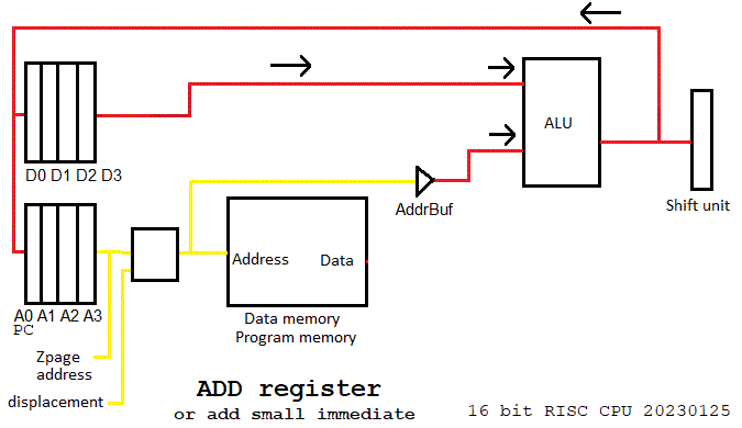
The same instructions can be done when the operand comes from an address register instead of from memory.
- MOV: The ALU can transfer addressregister+displacement to a register. This is done by forcing the data register output to zero and set the ALU operation to ADD. (The carry-output of the 4-bit displacement adder is routed to the main ALU where it is added to the result. So there is no need for alignment of the address register contents). This setup is used to add a small number to an address register.
- BRC / BRNC: Every MOV instruction can be conditional. A small number can conditionally be added to register A0 (the PC), providing conditional branches. The assembler generates long jumps but will use a near branch if possible (Long jumps can also be conditional).
- ADD: An address register can be added to any data register. A data register can also be added to an address register, but in this case the number of the source data register must be the same as the number of the destination address register. So ADD D2,A2 is possible but ADD D2,A3 is not possible.
- MOV: A data register can be moved to an address register by setting the zpage-address to zero and set the ALU to ADD. This will add 0 to the data register and put the result in the address register. The number of the source data register must be the same as the number of the destination address register. So MOV D2,A2 is possible but MOV D2,A3 is not possible. Of course, you can also add a small number in the same instruction by using a non-zero zpage-address.
This picture also shows that a Zpage address can be routed directly to the ALU. This provides the 8-bit immediate operand mode. This immediate mode can be used with all main instructions: MOV, MOVC, ADD, NOR.
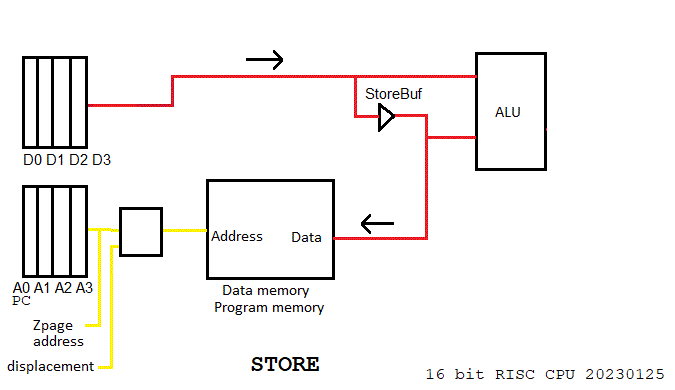
Finally, storing a data register is straightforward. There are instructions for store-word and store-byte. An address register can be stored by first moving it to a data register.
Note that the output of the ALU is also written back to the stored register (not shown here) because this effect is not suppressed in the current version. Since the data register contents is present on both ALU inputs, the dataregister will be added to itself. This is used in the SHL (shift left) instruction.
Several topics will be discussed later:
- incrementing the PC
- carry handling
- subroutines
- loading the upper 4 bits of address registers
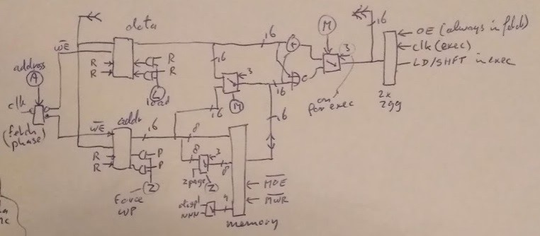
I can already uncover a bit more by showing my nice drawing (it is from an early version and no longer accurate):
Discussions
Become a Hackaday.io Member
Create an account to leave a comment. Already have an account? Log In.