 land-boards.com
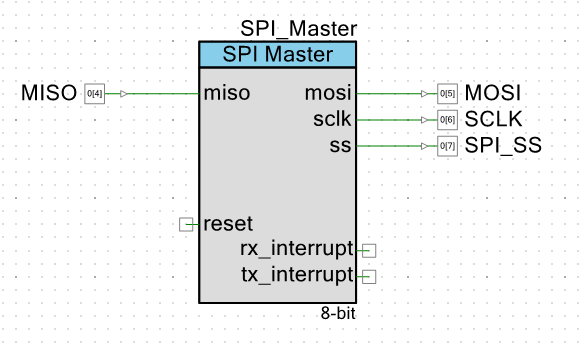
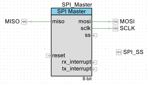
Created a SPI_Master in the PSoC TopDesign.cysch file:
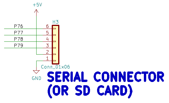
PCB Schematic
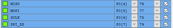
PSoC pin list
| Signal Name | PSoC Pin | H3 pin |
| MISO | 76 | H3-6 |
| MOSI | 77 | H3-5 |
| SCK | 78 | H3-4 |
| SS | 79 | H3-3 |
| Power | +5V | H3-2 |
| Ground | GND | H3-1 |
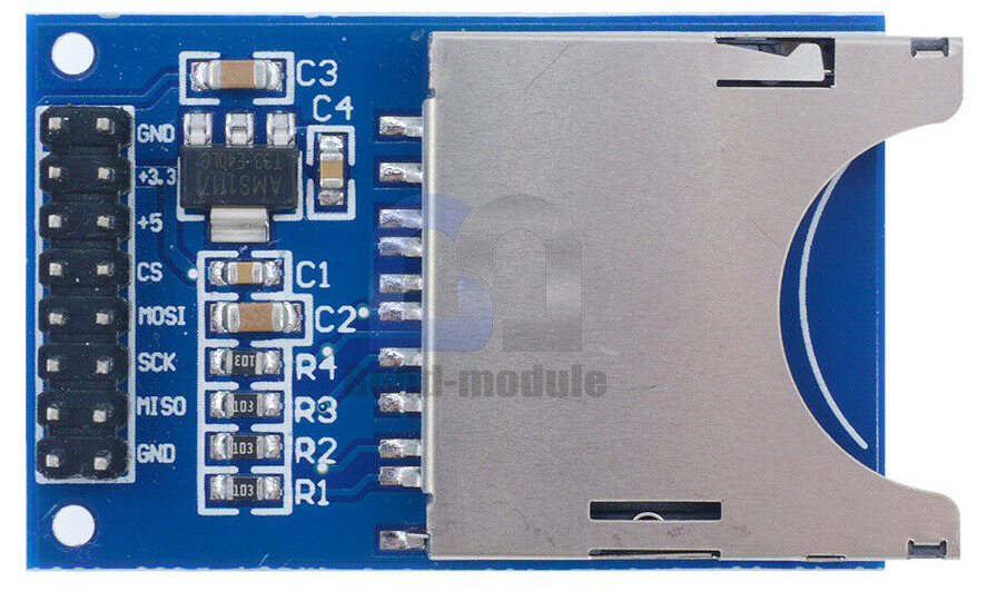
SD Card Adapter
These adapters are dirt cheap on Ebay. The extra row of pins allows debugging to be done easier.
The Z80 runs at 5V and SD Cards run at 3.3V. The adapter card has a voltage regulator to make 3.3V from the 5V. They don't typically have level shifters for the digital lines but they have 10K resistor in series with the 4 control lines so that should be OK.
Cable to connect adapter to Z80_PSoC connector.
Modified the schematic to make SS an output pin. That's because It needs to be held high for at least 74 clocks during initialization. Could be better to use a mux so that after initialization it could be switched to the in-built SPI interface.
Discussions
Become a Hackaday.io Member
Create an account to leave a comment. Already have an account? Log In.