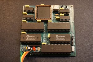
The 80C85 side is fairly basic, demux the address/data lines and turn a few signals from 808x into Z80 format. It's based on the Ancient Computing 8085 card design except that interrupts are instead routed to one of the RST x.5 lines so they actually work.
The MMU is nothing more than a latch at 0xFF that generates two sets of A16-A19 bits and a 4bit 2 way mux driven from a 3 input and gate (0000-DFFF/E000-FFFF) to select the memory used. At boot time the reset line sets the bits to 0 so the system powers up with the memory card ROM mapped for the full 64K and the boot ROM then moves to RAM.
Tested to the full 8MHz with a Tundra 80C85. It works fine that way but the CF adapter only works reliably at lower speeds. The PPIDE adapter which produces proper IDE timings unlike the CF hack works reliably at 8MHz.
ROM firmware, Fuzix and CP/M 3 are on github.
 EtchedPixels


 Ted Fried
 Eric Wright