-
Addressing Modes
10/16/2019 at 14:37 • 0 commentsModern processors have a wide variety of addressing modes which give the processor its flexibility and also complexity.
The very early processors, before about 1970 had far fewer addressing modes - which resulted in them being more challenging to program, as it would take several operations to achieve simple addressing operations.
I'm hoping to reach a balance between programability and complexity - and this will be down to choosing the most useful addressing modes - and finding an easy way to implement them in hardware.
The various addressing modes evolved over the decades with each new generation of machine.
Originally a Load-Store architecture was chosen for its simplicity, and the very fact that it didn't need expensive registers or a complex instruction set. This made it popular in the 1960s when hardware (transistor based) was still very expensive. At first, the only addressing mode was memory direct - where the address of the memory to be accessed was embedded as a bit-field within the instruction word. This severely restricted the span of memory that could be addressed to a small page of bytes, or meant that the instruction word-length had to be very long.
The next innovation was to use a level of indirection. Whilst you could only directly address a page of say 128 words, with indirection you could access a location of memory on the page that contained the absolute 12-bit address of the memory that you actually wanted to address. This method greatly increased the usefulness of the machine - without over-increasing the complexity of the hardware. That's why indirect memory addressing arrived with the early minicomputers of the mid-1960s, such as the best selling PDP-8 which initially could access 4096 words of memory using this technique.
Suite-16 uses 16 general purpose 16-bit registers, and this gives it a lot more capability than the traditional Load-Store architectures of the past. The registers may be considered to be a few words of memory that are close coupled to the ALU and can be accessed within the same ALU cycle - without having to address slower external memory. By the late 1960s new 16-bit minicomputers were appearing on the market - such as the PDP-11 and the Data General Nova and were starting to make heavy use of multi-register architectures. The PDP-11 had 8 general purpose registers, whilst the DG Nova had four accumulators, any of which could be the operand source or destination.
A description of the DG Nova ISA is here http://users.rcn.com/crfriend/museum/doco/DG/Nova/base-instr.html
So with locally available registers, you can either use the register's contents directly as the operand, or indirectly, by using it as the ad dress of where the operand is stored. This simple innovation gives us two of the most commonly used addressing modes:
Register Direct
Register Indirect
On Suite-16 I intend to use bit 14 of the instruction register to indicate whether to use direct or indirect addressing modes. Bit 12 of the Instruction register will signify whether the operation is a Load or Store operation.
The next useful addressing mode is indexed addressing. Here a register Rn can be used to form a base address, which can be augmented by a value X. The memory address that we access is given by (Rn + X) By incrementing X we can successively index into a table of data. Indexing is often used to select the nth item from a table of data. Sometimes however X is held constant and it is the value in Rn which is incremented (or decremented).
Indexed Addressing is often denoted X(Rn) - which signifies that the address held in Rn is modified by X. In Suite-16 we have the 8-bit payload encoded into the lower byte of the Instruction Register. This is an ideal place to locate the index X. If X=0 then the value of Rn goes unmodified.
A close cousin of Indexed Addressing is Symbolic Addressing. Here it is the PC that is modified by X forming the effective address (PC+X). If the PC is a general purpose register then Indexed mode X(PC) is the exact equivalent. Symbolic Addressing provides a convenient way to create look-up tables.
There are times that you wish to perform program branches or sub-routine calls, over the full addressing range of the memory. Whilst an 8-bit constant X can be used to provide short branches or calls within the same page of memory, by adding X to the PC, long Calls or Branches will require the PC to be reloaded with a completely new 16-bit value. As there is no room in the current instruction to package a 16-bit value it has to follow on in the next memory location. The word following the instruction contains the absolute address - and for this reason the mode is called Absolute Addressing - often denoted in assembly language as &ADDR.
There remains at least two more useful addressing modes, which came in to popularity with the PDP-11. They are useful for accessing stack structures - where the contents of the register is a pointer to an address in the stack - otherwise known as a Stack Pointer or SP. Sometimes there is a dedicated SP register that solely has access to the stack, but in an architecture with several general purpose registers, any one of them could be used to point to a stack, and several separate stacks could thus be created within memory.
Stacks operate on a last-in, first-out principle, and the only item on the stack which is accessible to the system is the item on the Top of Stack, which the stack pointer currently points to - sometimes called TOS. For historical reasons of operational convenience, stacks often originate in high-memory and grow downwards. The two operations that access the stack are called PUSH and POP.
You PUSH data (from the accumulator) onto the stack by first decrementing the stack pointer so that it points to the new Top of Stack (the next free location) and then you store the data. When you POP an item off the stack and load it back to the accumulator, you increment the stack pointer so that it points to the new item which is the Top of Stack. This process is sometimes referred to as Post Increment and Pre Decrement. No data is overwritten or moved, just the value in the stack pointer changes.
To help automate the stack operations, it is convenient to have an addressing mode that has an auto increment or auto decrement indirect mode.
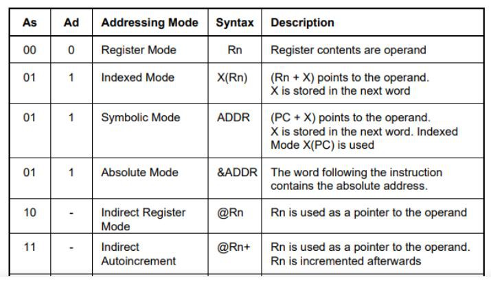
![]()
The table above conveniently summarises the Addressing Modes available on the MSP430 processor. Most of these should be achievable on the Suite-16 design.
-
Simulating the Instruction Set
10/16/2019 at 11:22 • 0 commentsSimulating the Instruction Set
Simulation is a powerful tool, and for a simple processor it is relatively quick to right some C code to give you confidence that your instruction set is doing what it is supposed to.
A simple processor may be simulated in fewer than a hundred lines of C code - and once you have implemented the basic model, you can begin to optimise the instruction set, adding and removing instructions until you think you have a useful set.
The most basic of simulators sets up an array of 16-bit unsigned integers in memory and this is where you need to place your instructions, one after the other, as they would exist in the program memory of the simulated processor. I have chosen to express this array as hexadecimal digits, because it's so much easier to work with hex instruction mnemonics on Suite-16.
#define MEMSIZE  1024
int M[MEMSIZE] = {

        0x1100,     // SET R1, 0x10
        0x0010,
        0x2100,     // LD AC, R1
        0xD000,     // DEC AC
        0x0103,     // BNZ 03
        0x1000,     // SET AC, 0x20
        0x0020,
        0xD000,     // DEC AC
        0x0107,     // BNZ 07
        0x0000,     // BRA 00
This very simple example executes a couple of down counters, testing the DEC instruction and conditional branching BNZ
Hand assembling anything more than a few instructions at a time can get tedious - so my next software task will be to create a tool, similar to an assembler which will make this process a lot easier.
I have chosen to simulate the Suite-16 cpu using an MSP430 microcontroller.
Firstly because it is a 16-bit cpu with a very orthogonal instruction set. Secondly it can easily be programmed using a derivative of the Arduino IDE called Energia, and thirdly it gives me access to 256kbytes of non-volatile FRAM memory and a microSD card. I view the Suite-16 cpu as a very much cut down version of the MSP430 but sharing a similar instruction set. Until I have actually built the TTL computer, the MSP430 might have to stand in as a hardware equivalent.
As Energia is a similer IDE package to Arduino, it should be possible to port the Suite-16 simulator to any microcontroller supported by Arduino. This includes everything from the humble ATtiny to the 400MHz STM32H743.
The simulation model is built around a simple switch-case structure - switching on the various values that form the op-code field.
 /* Opcode Execute */

    switch (op) {

    case 0x0:   break ;
    case 0x1:   R[n]= M[PC] ; PC++     ; break ; /* SET */
    case 0x2:   R[0] = R[n]            ; break ; /* LD */
    case 0x3:   R[n] = R[0]            ; break ; /* ST */
    case 0x4:   R[0] = M[pointer]      ; break ; /* LD@ */
    case 0x5:   M[pointer] = R[0]      ; break ; /* ST@ */
    case 0x6:   R[0] = M[pointer]      ; R[n]= R[n]-1 ; break ; /* POP */
    case 0x7:   M[pointer] = R[0]      ; R[n]= R[n]+1 ; break ; /* PSH */
    case 0x8:   R[0] &= R[n]           ; break ; /* AND */
    case 0x9:   R[0] |= R[n]           ; break ; /* OR */
    case 0xA:   R[0] += R[n]           ; break ; /* ADD */
    case 0xB:   R[0] -= R[n]           ; break ; /* SUB */
    case 0xC:   R[n] != R[n]           ; break ; /* COM */
    case 0xD:   R[n] = R[n]-1          ; break ; /* DEC */
    case 0xE:   R[n] = R[n]+1          ; break ; /* INC */
    case 0xF:   R[0] ^= R[n]           ; break ; /* XOR */
    }
The code snippet above shows the first draft. REG[0] is the accumulator and R[n] is any of the general purpose registers R1 to R15.
Memory and Register Operations
Instructions 01 to 07 handle the loading and storing of the selected register from and to the accumulator, both with direct and indirect addressing. For the direct load and store operations the Accumulator can be loaded with the value in the designated register Rn, or the contents of the Accumulator can be stored in the register Rn.
Indirect addressing uses the contents of the register Rn to form the memory address for the word in memory M[pointer].
Push and Pop allow the accumulator to be deposited or retrieved from a stack structure addressed by the selected register Rn - which acts as a stack-pointer, and is automatically incremented or decremented after each stack operation.
ALU Operations.
The remainder of the operations 8x to Fx are arithmetical or logical instructions and will thus involve the ALU.
They will either be a two-operand instruction involving the accumulator and a register - such as ADD, SUB, CPR, AND, OR and XOR
or they will be a one-operand operation where the ALU is used to increment or decrement the value within a given register.
Class 0x Instructions
These are reserved for the program flow instructions such as Call, Return, JMP and the conditional branches.
The conditional branches can be handled with the following bit of code:
/* Conditional Branches */ A = REG[0] ; if (op == 0) { // It's an 0x branch - so test the accumulator against the following conditions // then load the PC with the address in the address field unsigned int cond = (IR & 0xf00) >> 8 ; // Extract the condition field switch (cond) { case 0x0: PC = addr ; break ; // BRA Branch Always case 0x1: if(A>0) { PC = addr ; } break ; // BGT Branch if Greater case 0x2: if(A<0) { PC = addr ; } break ; // BLT Branch if Less Than case 0x3: if(A>=0) { PC = addr ; } break ; // BGE Branch if Greater or Equal case 0x4: if(A<=0) { PC = addr ; } break ; // BLE Branch if Less Than or Equal case 0x5: if(A!=0) { PC = addr ; } break ; // BNE Branch if Not Equal to zero case 0x6: if(A==0) { PC = addr ; } break ; // BEQ Branch if Equal to zero case 0x7: break ; case 0x8: break ; case 0x9: break ; case 0xA: break ; case 0xB: break ; case 0xC: break ; case 0xD: break ; case 0xE: break ; case 0xF: break ; } -
More About the Instruction Set
10/16/2019 at 11:04 • 1 commentKey to the operation of the machine is the Instruction Set.
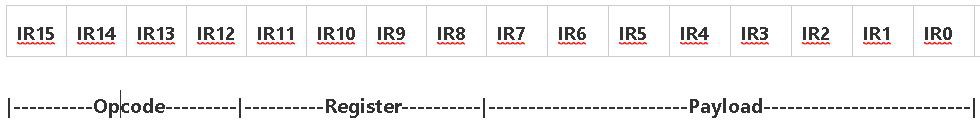
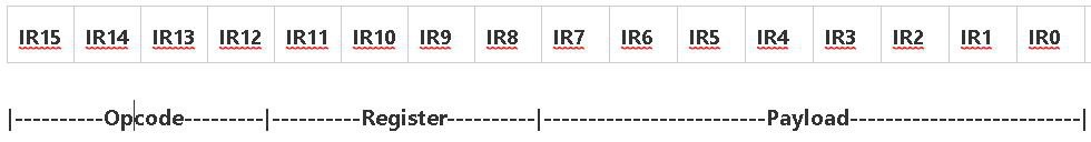
Suite-16 uses a 16-bit wide instruction word format which is separated into various bitfields.
The instruction exists as an 8-bit wide bytecode located in the upper byte of the Instruction Register IR15:8 and an 8-bit payload byte in IR7:0.
The Operation is encoded into the bitfield IR15:12, and the Register Rn is encoded into bitfield IR11:8.
![]()
Here is the Instruction Set as it currently stands:
/* Suite-16 Instructions Register OPS- 0n --- -- Non-Register Ops 1n SET Rn Set Constant Rn = @(PC+1) 2n LD Rn Load AC = Rn 3n ST Rn Store Rn = AC 4n LDI @Rn Load Indirect AC = @Rn 5n STI @Rn Store Indirect @Rn = AC 6n POP @Rn Pop AC AC = @Rn Rn = Rn - 1 7n PUSH @Rn Push AC @Rn = AC Rn = Rn + 1 8n AND Rn AND AC = AC & Rn 9n OR Rn OR AC = AC | Rn An ADD Rn Add AC = AC + Rn Bn SUB Rn Sub AC = AC - Rn Cn CPR Rn Compare AC = AC - Rn R13 = flags Dn DEC Rn Decrement Rn = Rn - 1 En INC Rn Increment Rn = Rn + 1 Fn XOR Rn XOR AC = AC ^ Rn Non-register OPS- 00 JMP 16-bit Target = @(PC+1) 01 BGT AC>0 Target = IR7:0 02 BLT AC<0 Target = IR7:0 03 BNE AC!=0 Target = IR7:0 04 BEQ AC=0 Target = IR7:0 05 BGE AC>=0 Target = IR7:0 06 BLT AC<=0 Target = IR7:0 07 BRA Always Target = IR7:0 08 CALL 16-bit Target = @(PC+1) 09 RET Return 0A Unassigned 0B Unassigned 0C Unassigned 0D Unassigned 0E Unassigned 0F Unassigned */![]()
Instruction Decoding
I have made some subtle changes to the order of the instructions, which I think may simplify instruction decoding.
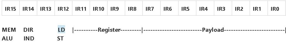
Firstly instructions that access memory or registers are in the lower half of the Opcode group when IR15 is zero.
Those that involve ALU operations are in the upper half of the Opcode group when IR15 is set.
Opcodes 0n to 3n all deal with the register direct, 4n to 7n all deal with the register indirect. This means that bit IR14 of the instruction register can be used to signify direct or indirect register addressing modes, when combined with the condition that IR15=0.
In a similar way, bit IR12 can be used to differentiate between operations that load the accumulator AC and those that store the Accumulator. IR12 becomes effectively a !RD/WR indication when combined with the condition IR15=0 and IR14=0
There is no real logical pattern to the ALU operations, except that I wanted some mnemonic value - A for Add, B for suB, C for Compare, D for Dec. It rather falls apart after that, except E could be for Exclusive OR.
I'm still not certain whether the Compare operation is really justified, after all it is really just a variant of subtraction.
Notes
There are at most 31 instructions, which can be divided into the following groups:
Register/Memory Transfer 7 instructions
Register/ALU Operations 8 instructions
Program Flow Control 10 Instructions
Unassigned 6 Instructions
With just 31 instructions, Suite-16 could qualify as being a mimimum instruction set computer - or MISC.
Instructions form 2 main groups - those that are Register Operations, and those that are Non-Register Operations
The Register Operations are further divided into Register/Memory ops and Register/ALU ops.
Register/Memory instructions form the basis of immediate, register direct and register indirect addressing modes. I have included a Push and Pop which supports Accumulator transfer to register indirect addressed memory combined with an auto-increment or decrement of the designated register.
The Register/ALU operations are defined entirely by the current capability of the ALU. Other operations may be possible - such as shift right, clear and complement, but hardware restrictions in instruction decoding will mean that these operations can only work on the Accumulator.
The non-Register Operations are mainly concerned with program flow, Branching, Conditional Branching, Call and Return.
Branching has a span of +/-128 addresses to either side of the current Program counter - with the Program Counter offset being contained in the lower 8-bits of the Instruction Register IR7:0.
Subroutine Call, and absolute Jump have an absolute address range of 16-bits - and the target address is contained in the next memory word at (PC+1).
So far the Call and Jump instructions do not use the lower 8-bits of the Instruction Register IR7:0. These unused bits could possibly be used to extend the addressing range to a full 24-bits, or 65,536 pages of 256 words. Paged memory has been around for a long time as a cost effective way of being able to address more memory - but without having to extend all of the data bus widths of the registers.
This is an intriguing concept for extending the scope of the whole machine. Memory is cheap these days - and the whole 16M x 16 could be populated for under $150.
Memory could be addressed as a linear model, consisting of 256 pages of 64K. This would be one way of partitioning the memory to support relatively few large applications - running in separate 64K pages. The other extreme is to have an object model - where memory supports a large number (64K) of small 256 word objects. This alternative arrangement may be useful for supporting modern object-oriented languages, CAD programs where objects drawn on the screen have their properties coded as separate objects in memory or for languages such as Forth - where each Forth Word, is coded into a small page of memory and addressed by a 16-bit pointer. Thanks to Roelh and his Kobold 2 project for explaining these different memory models https://hackaday.io/project/167605-kobold-k2-risc-ttl-computer/log/168785-accessing-memory
The last six instructions of the non-Register operations are currently unassigned. These will probably be used for Input/Output operations, manipulating the accumulator contents directly, or used in a similar manner to the PDP-8 OPR instructions which are used to control the hardware directly.
-
Hardware - Explaining the BitSlice Design
10/15/2019 at 22:14 • 0 commentsIn my last project log I discussed the instruction set for Suite-16, and actually found time to implement some of it in a C code simulator. This is an ongoing work in progress - and will be discussed in a future project log..
In this log, I'm going to attempt to clarify the hardware design and explain what is meant by a bitslice.
Bitslice design is a means of partitioning complex logic circuits into manageable modules. It has it's origins in the early 1960s and was used extensively in computers such as the PDP-8 (1965) and the Data General Nova (1969).
It's based on the premise that when you perform bitwise logic on multi-bit operands (say 8-bit or 16-bit) that each bit can be treated as a separate operation - with no dependencies to bits either side to the one that is being processed.
In short, if you wish to perform a 16-bit bitwise AND on two operands A and B, then you could do this with four identical circuits - each of which could AND four bits. By stacking four of these identical 4-bit AND modules next to each other, you can perform a 16-bit AND.
When it comes to arithmetic operations such as ADD and SUB - conveniently the manufacturers of TTL chips designed a 4-bit adder (usually the 74xx283). As a single IC this can add two, 4-bit numbers, with internal connections for the Carry signals from one bit to the next. If you take four of these chips and connect the CarryOut (CO) of the lesser stages to the CarryIn (CI) of the next stage - you can build up larger adder circuits for 8, 12 and 16-bit designs.
TTL first appeared in the early 1960s - demand driven by the aerospace and missile industry. Each IC was restricted to at most a few hundred transistors - medium scale integration or MSI. The designers of those early 74xx series logic devices tried to cram as much as they could into the much cheaper 14 pin and 16 pin packages. Later on, the devices became much cheaper and were widely adopted by the computer industry. Now, some 50 years later since the commercial introduction of affordable TTL (in about 1969) that so many of the useful functions cater for a 4-bit wordsize and are still all available today - packaged in a 16 pin DIL package.
This is all great news for the designers of TTL computers - even in 2019.
Some of the 4-bit wide 7400 series ICs that will be used in Suite-16:
74xx157 Dual 4-input multiplexer
74xx157 Quad 2-input multiplexer
74xx161 4-bit presettable binary counter
74xx173 Quad D-type flip flop
74xx193 4-bit synchronous binary up/down counter
74xx194 Universal 4-bit bidirectional shift register
74xx219 4-bit x 16 word RAM
74xx283 4-bit binary adder
74xx670 4 x 4 register file
A Bitslice ALU based on Multiplexers
At the heart of any processor is the Arithmetic and Logic Unit or ALU. As its name suggests, it performs arithmetical and logic operations on usually two binary operands. The ALU can be very simple - such as the PDP-8 which offered just ADD and AND of a memory operand with the Accumulator. It also allowed the Accumulator to be inverted, and a carry bit added so that instructions such as subtraction could be synthesised. With inversion and bitwise AND, all of the other logic operations could also be created from small macros of instructions.
The ALU of the PDP-8 was designed at a time before integrated circuits were widely available and used a discrete diode-transistor logic called DTL. Transistors were very expensive (about $20 in today's equivalent), and so were used very sparingly, with the diodes supplying much of the AND-OR logic. The PDP-8 was one of the first commercial bitslice designs, with 12 circuit boards stacked side by side in the rack - each of which contained 1 bits-worth of circuitry.
With the arrival of cheaper TTL, you could afford to design a more sophisticated ALU - and by the late 1960s you could buy a complete, multifunction 4-bit ALU - the 74181, packaged in a 24 pin package. The 74181 was the computer design engineer's dream - and was widely used in minicomputers and controllers where multi-bit computation was needed.
Unfortunately the 74181 has been obsolete for many years, and is impractical to use for a new design. However there is a clever means to obtain almost all of the capability of the 74181 using a combination of 4-input multiplexers and an adder.
The proposed ALU will have the following instructions ADD, SUB, AND, OR, XOR with extensions for INV, INC, DEC and SHR (shift-right).
I am deeply indebted to Dieter Muller of 6502.org for the design of the ALU. More than a decade ago, Dieter described a way of using low cost multiplexer ICs to create a very versatile ALU.
Dieter has documented many years of TTL design from his own experience - and his pages on ALU design using multiplexers describes them as the "Tactical Nuke" of Logic Design.
http://www.6502.org/users/dieter/a1/a1_4.htm
I won't go into the full details here, partly because I will cover them in full in a later post - and also because Dieter more than adequately describes them on his own site (well worth the read). Needless to say, his design has been widely adopted as the coolest way to make a versatile ALU from simple TTL chips.
Suite-16 has been greatly inspired by Marcel van Kervinck's Gigatron, which uses an ALU based on Dieter Muller's design. Suite-16 embraces this design and packages it up into a form suitable for bitslice design.
-
Exploring the Instruction Set - Architecture
10/15/2019 at 17:11 • 0 commentsSuite-16
The inspiration for this project was to design a 16-bit TTL computer loosely based on Steve Wozniak's 16-bit virtual cpu "Sweet-16".
It written in 6502 assembly language to augment the Apple II when performing 16-bit operations. Sweet-16 is well documented here:
http://www.6502.org/source/interpreters/sweet16.htm#Instruction_Descriptions_
Wozniak's Sweet-16 created 16 virtual 16-bit registers within 32 bytes of the 6502 zero page memory.
He implemented a 16-bit virtual machine to manipulate these registers, and handle 16-bit data using a simple instruction set.
The instructions exist as bytecodes which could be interwoven within 6502 assembly language.
The instruction set was not only simple but elegant - and trivial to remember the assembly codes. This got me thinking whether it might be a suitable candidate for a real 16-bit cpu - implemented in TTL hardware.
One major restriction of Sweet-16 compared to other register machines, is that register R0 takes the role of the accumulator AC, and almost all operations involve the accumulator and one other register. It is not possible to do register to register operations - except through the accumulator. This restriction reduces the complexity of the ISA as there is no need for source and destination bit-fields - because the accumulator is usually always the destination. This reduction in complexity is also reflected in the hardware - because there is no need to include hardware to select source and destination registers, or to allow the contents of one register to be moved to another.
This overall simplification gives me a greater confidence that I can actually design and build such a machine - and more to the point implement it in a reasonable number of TTL ICs. I have set a limit of 80 to 100 ICs and this should result in a manageable and more modest design both in hardware and cost.
The first task was to analyse the Sweet-16 instruction set and extract the parts that could be useful to a 16-bit TTL computer.
Wozniak's Sweet-16 Instruction set is summarised in the following table:
Register OPS-

     1n        SET       Rn     Constant  (Set)
     2n        LD        Rn     (Load)
     3n        ST        Rn     (Store)
     4n        LD        @Rn    (Load Indirect)
     5n        ST        @Rn    (Store Indirect)
     6n        LDD       @Rn    (Load Double Indirect)
     7n        STD       @Rn    (Store Double Indirect)
     8n        POP       @Rn    (Pop Indirect)
     9n        STP       @Rn    (Store POP Indirect)
     An        ADD       Rn     (Add)
     Bn        SUB       Rn     (Sub)
     Cn        POPD      @Rn    (Pop Double Indirect)
     Dn        CPR       Rn     (Compare)
     En        INR       Rn     (Increment)
     Fn        DCR       Rn     (Decrement)

Non-register OPS-

     00        RTN              (Return to 6502 mode)
     01        BR        ea     (Branch always)
     02        BNC       ea     (Branch if No Carry)
     03        BC        ea     (Branch if Carry)
     04        BP        ea     (Branch if Plus)
     05        BM        ea     (Branch if Minus)
     06        BZ        ea     (Branch if Zero)
     07        BNZ       ea     (Branch if NonZero)
     08        BM1       ea     (Branch if Minus 1)
     09        BNM1      ea     (Branch if Not Minus 1)
     0A        BK               (Break)
     0B        RS               (Return from Subroutine)
     0C        BS        ea     (Branch to Subroutine)
     0D                         (Unassigned)
     0E                         (Unassigned)
     0F                         (Unassigned)
Register Operations
Sweet-16 forms a reasonable starting point for an ISA, but remember that it was intended for a 16-bit virtual machine running on 8-bit hardware with byte-wide memory.
As I will be using 16-bit wide memory, some of the instructions slots are redundant, and these can be replaced with operations which better match the capabilities of the ALU - for example the inclusion of AND, OR and XOR instructions. I also wish to include instructions that correctly PUSH and POP the accumulator incrementing or decrementing the register that is acting as the stack-pointer.
16-Bit Instruction Word Width
![]()
The other major deviation from Woz's bytecode implementation, is that the Instruction Register width is now 16-bits.
I intend to use the upper byte very much as its used in Sweet-16 with 4 bits to define the operation and 4 bits to define the register.
I believe that this makes remembering the assembly code a trivial matter - and I am all for making assembly code more human readable.
This then leaves the lower byte of the instruction as a "payload" byte. This might be used as an 8-bit literal, a small constant, an offset to modify a register or a means of addressing a zero page memory address.
It is the use of this payload byte, which I believe will give the instruction set its flexibility. It will open-up additional addressing modes that were not part of the original Sweet-16 idea.
Zero Page addressing became popular with the advent of the minicomputer in the mid-1960s and the idea was continued with the early microprocessors such as the 6502. The memory locations within the zero page are accessible directly from the address bits encoded into the lower bits of the instruction word, within the one instruction cycle. This meant much faster access - and the zero page was heavily used for holding frequently used variables. Having a rapid access to the zero page locations meant that they were almost treated as pseudo-registers, making up for the lack of real registers in some architectures.
It is intended that Suite-16 will have both a collection of general purpose registers, and a zero page addressing mode to allow for the greatest flexibility from the least hardware.
Addressing memory as 16-bit words may not be the most efficient use of memory - especially where byte, ASCII and text operations are concerned. This will be a limitation of the design, but allowing a simplification to the hardware.
I am planning the means to provide a byte-swap mechanism in hardware - this may improve the flexibility for byte operations.
Non-Register Operations.
The non-register operations in Sweet-16 are mainly concerned with program flow and branching. I intend to keep this arrangement - particularly for the first eight of the 0x instructions, 00 to 07. These will be the conditional branch instructions, and can be decoded from the three lower bits. As my ALU is based on that used in the Gigatron TTL computer - the conditional branch mechanism will be virtually identical.
Short branches of up to +/-128 locations of the current PC can be performed by modifying the PC with the signed 8-bit value included in the payload byte. This is fairly standard practice on a number of common processors.
Long branches or calls will pick up the full 16-bit destination address from the next full 16-bit instruction. PC = (PC+1)
This leaves instructions 08 to 0F unassigned and I currently have a plan to use those to operate on the accumulator, such as shift operations, clear and complement accumulator, and a means of handling Input and Output. Other operations such as loading commonly used short constants - such as 0, 1, 2, 4, 8, and -1 (FFFF) will be coded here. These operations are inspired by the OPR instructions in the PDP-8 and the constant generator in the MSP430.
The non-register 0x operations also have the 8-bit payload byte attached to them. This could be also be used for zero page addressing or possibly allowing up to 256 I/O ports communicate with the accumulator.
Suite-16
Suite-16 is a 16-bit cpu built entirely from TTL. It is a personal exploration of how hardware and software interact.