This post is a followup of the Improved Address Register post.
We have identified 4 asynchronous actions:
- Publish MSB to data bus: -msb-out, asynchrounous
- Publish LSB to data bus : -lsb-out, asynchrounous
- Publish value to Adress bus : -add-out, asynchrounous
- Clear value (reset) : -clear, asynchrounous
and 4 synchronous actions:
- load MSB from data bus : -msb-in, on clock rising edge
- load LSB from data bus : -lsb-in, on clock rising edge
- Increment value : -inc, on clock falling edge (see note)
- decrement value : -dec, on clock falling edge (see note)
However, the 74HCT193 does not provide a clock entry, therefore it has to be built with an NAND gate to synchronise the action signal and the clock. So when activating the INC action, NANDed with the clock, will provide a HIGH-LOW-HIGH transition synchronous with the clock.

NOTE : the 74HCT193 has a strange behaviour in a way : it needs the clock inputs to be HIGH to count, but it counts on the rising edge. So, in order for intance to have a count UP you will need :
- CPDw to be HIGH
- CPUp which was HIGH to first go LOW and then go HIGH.
This means that the couting will not take place on the clock rising edge but on the clock falling edge after the NAND gate.
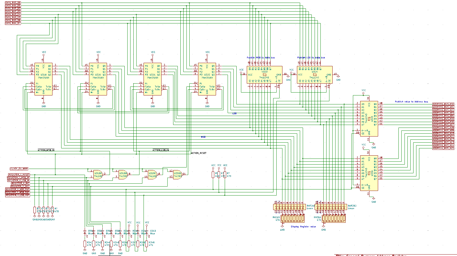
The 4 NAND gates provides 4 clock-synchronous action signals to control the 74HCT193. We need 4 of these to provide 16 bits. The increment and decrement counters are daisy chained to provide the counting capability :

The reset pin (Mr in the diagram) is just the same signal for all four chips.
The Pl (parallel load) signal is however distinct because we need to be able to load either the lower 8 bits (LSB) or upper 8 bits (MSB).
Therefore the output of the NAND gate for the signal REGISTER_X_MSB_IN is routed to the Pl pin of the two left chips and the output of the NAND gate for the signal REGISTER_X_LSB_IN is routed to the Pl pin of the two right chips.
Finally, for the output, we need to :
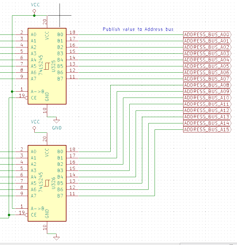
- publish the full address (16 bits) to the address bus. This is done using two 74HCT245 bus drivers with only one publish signal connected to both REGISTER_X_ADD_OUT (active low):

- publish the upper 8 bits to the data bus. This is done using one 74HCT245 bus driver driven by the REGISTER_X_MSB_OUT (active low) signal
- publish the lower 8 bits to the data bus. This is done using one 74HCT245 bus driver driven by the REGISTER_X_LSB_OUT (active low) signal
Overall, there are 9 chips to perform all these features:

In this diagram we added:
- 2 LED bargraphs to display the current value of the register
- 8 pullup/pulldown resistors to ensure that even if not connected the actions signals do not perform any action
- 8 signal LEDs to display the action sigals
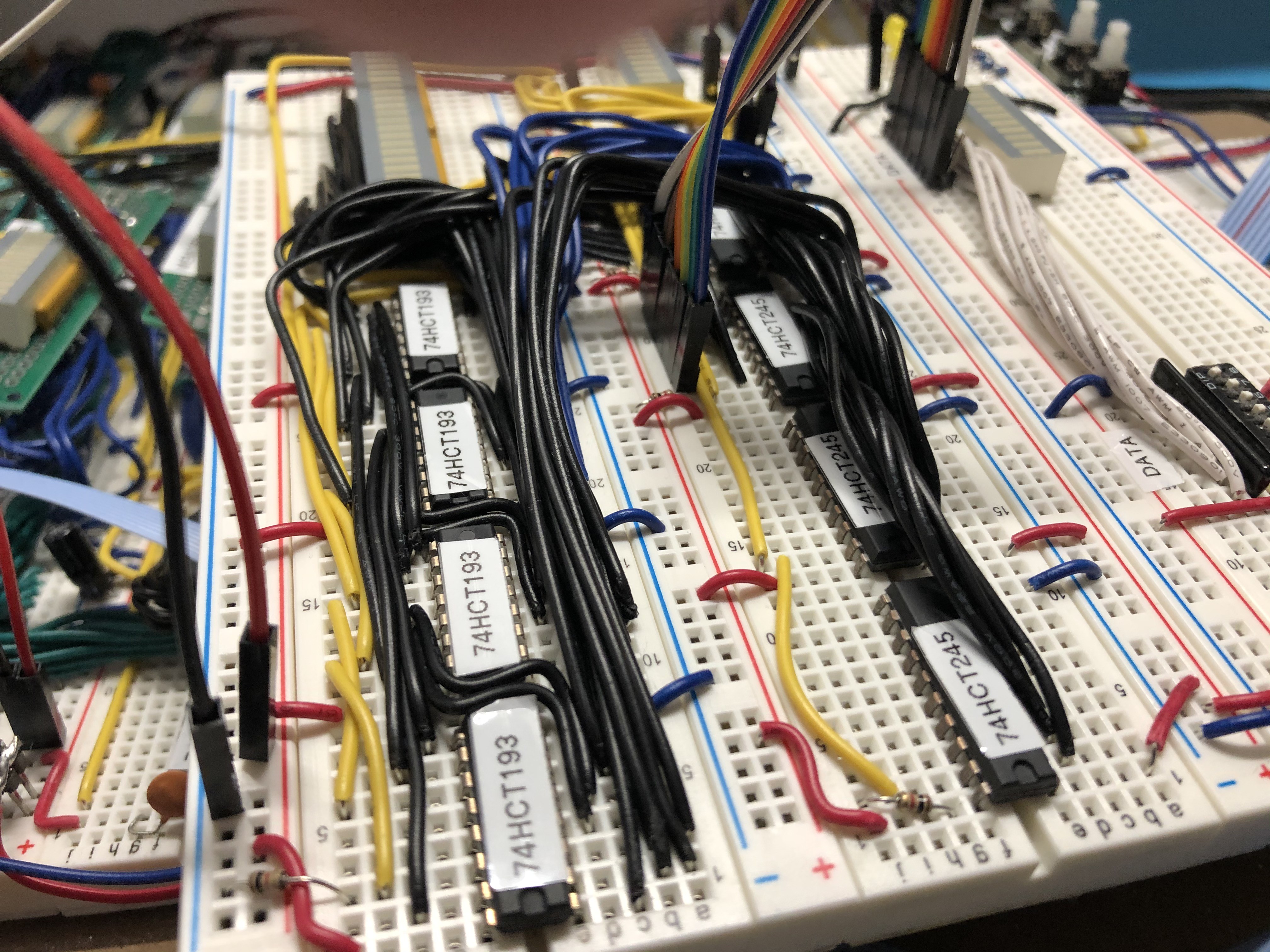
Here is the prototype using breadboards. It's a bit messy because the 74HCT193 have a very weird pinout.

The prototype has been tested and is working perfectly. Max tested frequency is 4 Mhz.
The next step is to build a PCB for this Register and connect it to a bus backplane. We will need 4 of these.
 Ced
Ced
Discussions
Become a Hackaday.io Member
Create an account to leave a comment. Already have an account? Log In.