References
Article: https://www.pcbway.com/blog/technology/DC_to_DC_Buck_Converter_Adjustable__97__Efficient__3A.html
[1]: https://www.mouser.com/datasheet/2/277/MP2315_r1.01-478439.pdf
[2]: https://componentsearchengine.com/part.php?partID=930350
[3]: https://www.samacsys.com/altium-designer-library-instructions
A tiny DC to DC buck converter board is useful for many applications, especially if it could deliver currents up to 3A (2A continuously without heatsink). In this article, we will learn to build a small, efficient, and cheap buck converter circuit.
[1]: Circuit Analysis
Figure 1 shows the schematic diagram of the device. The main component is the MP2315 step-down buck converter.
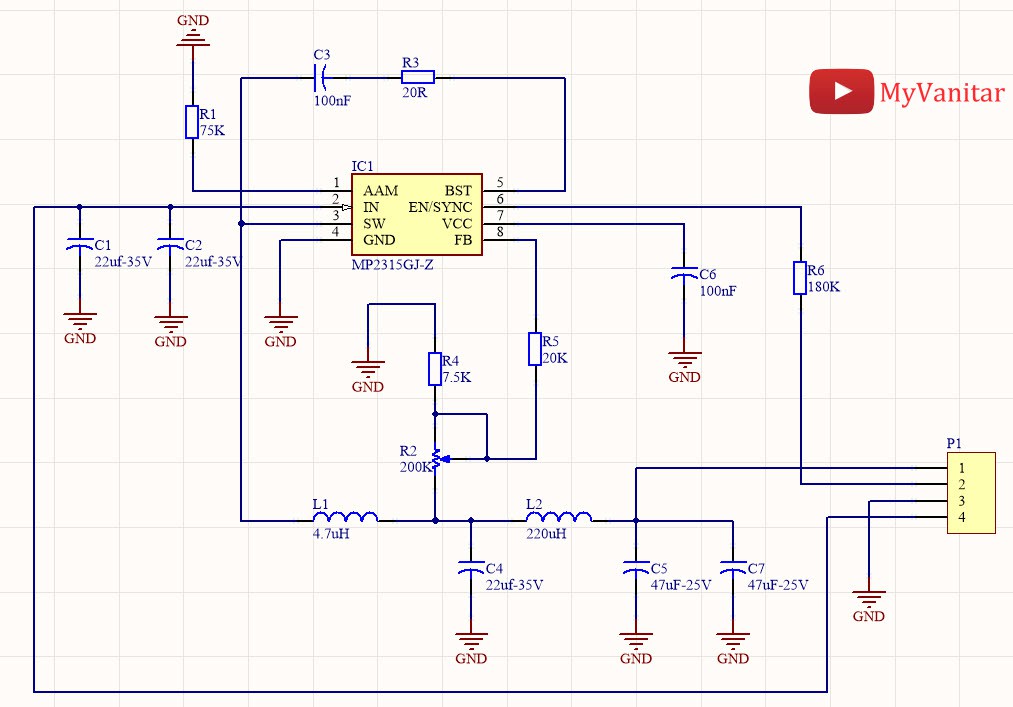
Figure 1, Schematic diagram of the DC to DC buck converter
According to the MP2315 [1] datasheet: “The MP2315 is a high frequency synchronous rectified step-down switch-mode converter with built-in internal power MOSFETs. It offers a very compact solution to achieve 3A continuous output current over a wide input supply range with excellent load and line regulation. The MP2315 has synchronous mode operation for higher efficiency over output current load range. Current mode operation provides a fast transient response and eases loop stabilization. Full protection features include OCP and thermal shut down.” Low RDS(on) allows this chip to handle high currents.
C1 and C2 are used to reduce input voltage noises. R2, R4, and R5 build a feedback path to the chip. R2 is a 200K multiturn potentiometer to adjust the output voltage. L1 and C4 are the essential buck converter elements. L2, C5, and C7 make an additional output LC filter that I added to reduce the noise and ripple. The cut-off frequency of this filter is around 1KHz. R6 limits the current flow to the EN pin. The R1 value has been set according to the datasheet. R3 and C3 are related to the bootstrap circuit and determined according to the datasheet.
Figure 2 shows the efficiency vs output current plot. The highest efficiency for almost all input voltages has been achieved at around 1A.
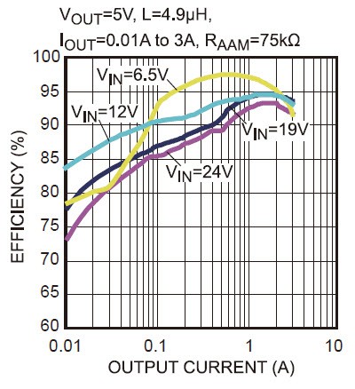
Figure 2, Efficiency vs output current
[2]: PCB Layout
Figure 3 shows the designed PCB layout. It’s a small (2.1cm*2.6cm) two layers board.
I used the SamacSys component libraries (Schematic symbol and PCB footprint) for the IC1 [2] because these libraries are free and more importantly, they follow the industrial IPC standards. I use the Altium Designer CAD software, so I used the SamacSys Altium plugin to directly install the components libraries [3]. Figure 4 shows the selected components. You can search and install/use the passive components libraries as well.
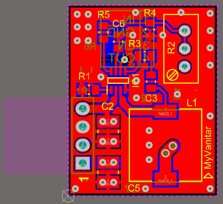
Figure 3, PCB layout of the DC to DC buck converter
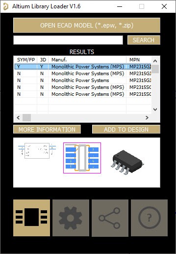
Figure 4, Selected component (IC1) from the SamacSys Altium plugin
This is the last revision of the PCB board. Figure 5 and figure 6 show 3D views of the PCB board, from the top and bottom.
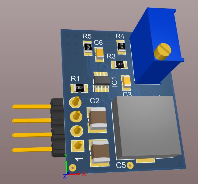
Figure 5, A 3D view of the PCB board (TOP)
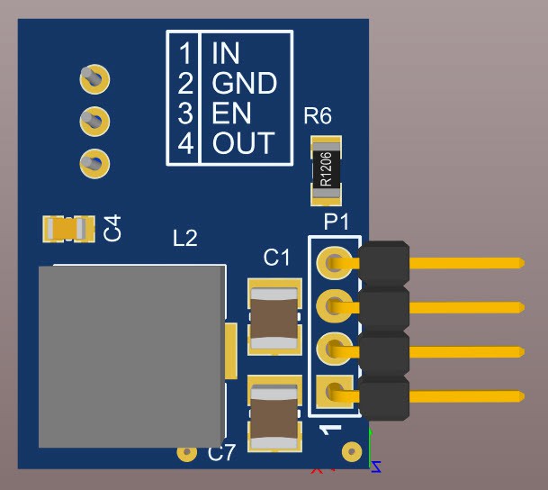
Figure 6, A 3D view of the PCB board (Bottom)
[3]: Construction and Test
Figure 7 shows the first prototype (first version) of the board. The PCB board has been fabricated by the PCBWay, which is a high-quality board. I had no problem with soldering whatsoever.
As it is clear in figure 8, I have modified some parts of the circuit to achieve lower noise, so the provided Schematic and PCB are the latest versions.

Figure 7, The first prototype (an older version) of the buck converter
After soldering the components, we are ready to test the circuit. The datasheet says that we can apply a voltage from 4.5V to 24V to the input.
The main differences between the first prototype (my tested board) and the last PCB/Schematic are some modifications in the PCB design and component placement/values. For the first prototype, the output capacitor is only 22uF-35V. So I changed it with two 47uF SMD capacitors (C5 and C7, 1210 packages). I applied the same modifications for the input and replaced the input capacitor with two 35V rated capacitors. Also, I changed the output header’s location.
Since the maximum output voltage is 21V and capacitors are rated at 25V (ceramic), then there should not be a voltage rate problem, however, if you have concerns regarding the capacitors’ rated voltages, simply reduce their capacitance values to 22uF and increase the rated voltages to 35V. You can always compensate this by adding extra output capacitors on your target circuit/load. Even you can add a 470uF or 1000uF capacitor “externally” because there is no enough space on the board to fit any of them. Actually, by adding more capacitors, we decrease the cut-off frequency of the final filter, so it would suppress more noises.
It is better that you use the capacitors parallelly. For instance, use two 470uF in parallel instead of one 1000uF. It helps to reduce the total ESR value (the parallel resistors rule).
Now let’s examine the output ripple and noise by using a low-noise front end oscilloscope such as Siglent SDS1104X-E. It can measure voltages down to 500uV/div, which is a very nice feature.
I soldered the converter board, in accompany with an external 470uF-35V capacitor, on a small piece of DIY prototype board to test the ripple and noise (figure 8)
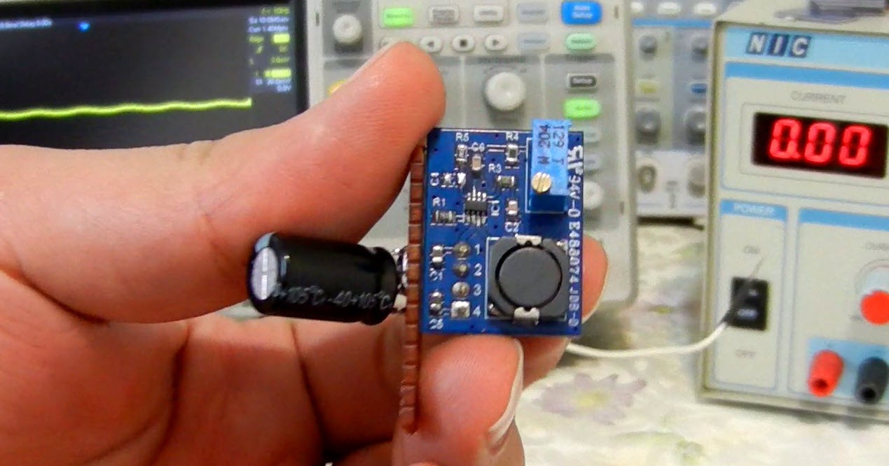
Figure 8, The converter board on a small piece of DIY prototype board (including a 470uF output capacitor)
When the input voltage is high (24V) and the output voltage is low (5V for instance), the maximum ripple and noise should be generated because the input and output voltage difference is high. So let’s equip the oscilloscope probe with a ground-spring and check the output noise (figure 9). It is essential to use the ground-spring, because the ground wire of the oscilloscope probe can absorb a lot of common-mode noises, especially in such measurements.

Figure 9, Replacing the probe’s ground wire with a ground-spring
Figure 10 shows the output noise when the input is 24V and the output is 5V. It should be mentioned that the converter’s output is free and has not been connected to any load.

Figure 10, Output noise of the DC to DC converter (input =24V, output = 5V)
Now let’s test the output noise under the lowest input/output voltage difference (0.8V). I set the input voltage to 12V and the output to 11.2V (figure 11).
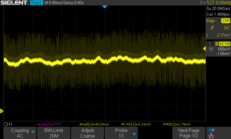
Figure 11, Output noise under the lowest input/output voltage difference (input=12V, output=11.2V)
Please note that by increasing the output current (adding a load), the output noise/ripple increases. This is a true story for all power supplies or converters.
[4] Bill of Materials
Figure 12 shows the project’s bill of materials.
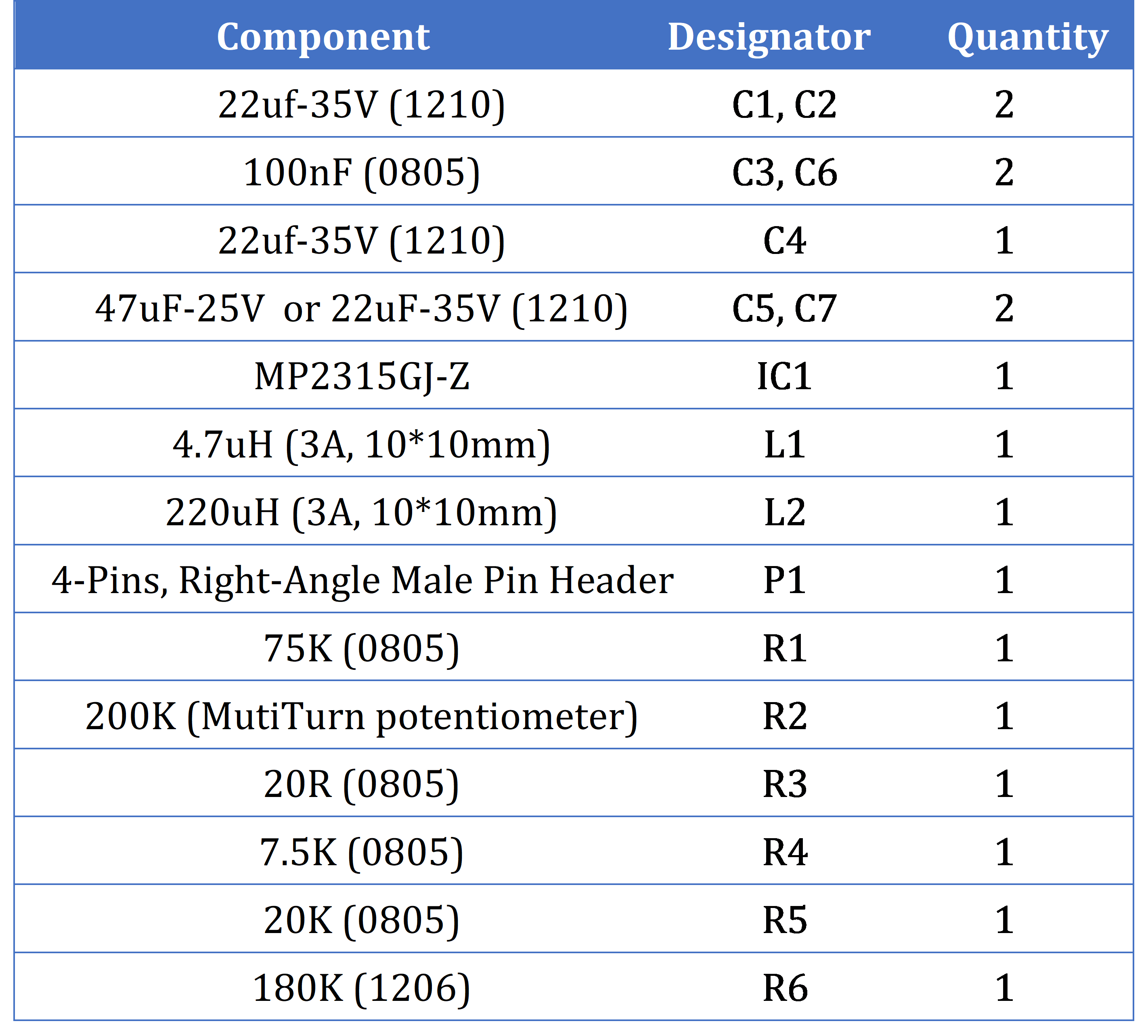
Figure 12, Bill of materials
 hesam.moshiri