 Jared Sanson
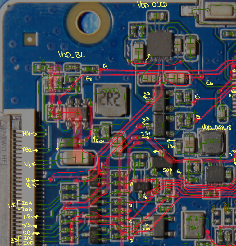
To start reverse-engineering the circuit behind this board, I started by taking photos of the bottom and top layers, and inking over with my Surface:
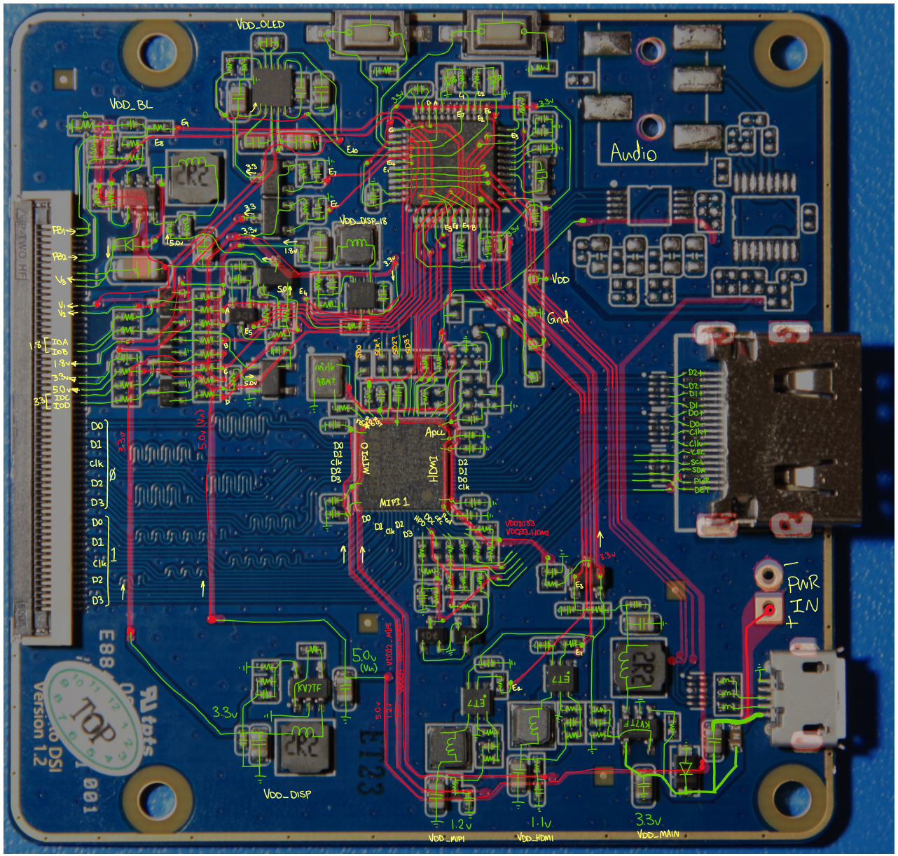
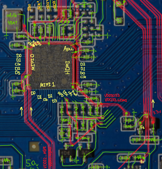
MIPI-HDMI Bridge Chip
You can see that the connector on the right does indeed support two MIPI channels, each consisting of 4 data pairs & 1 clock pair. The MIPI bridge chip is connected to the MCU via I2C, and there is minimal support circuitry (only a crystal, a few buck regulators, and some passives for the PLL).
Main Buck Regulators
On the bottom-right you can see the main buck regulators which supply power to the MIPI bridge chip. 5.0V is fed onwards to the display buck regulators elsewhere on the PCB.
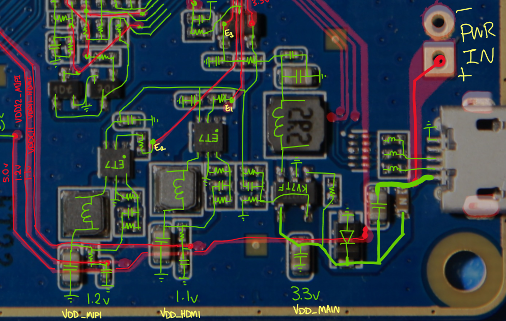
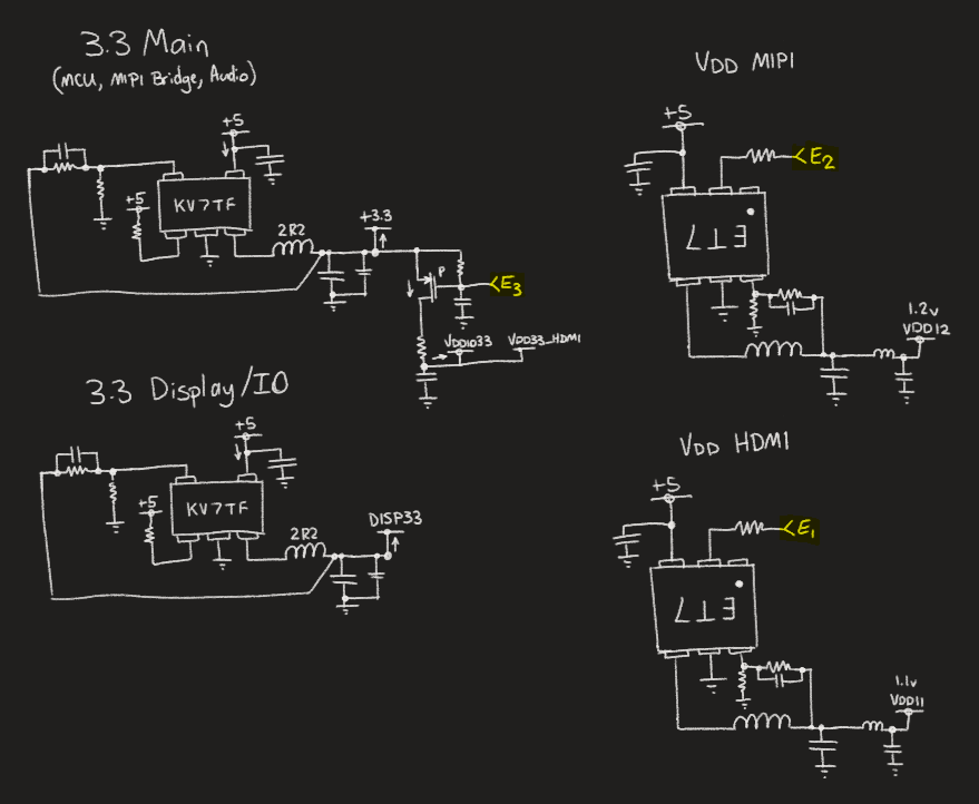 E1 controls the 1.1v supply for the MIPI bridge (VDDC11, VDD11_HDMI)
E2 controls the 1.2v supply (VDD12_MIPI)
E3 controls the 3.3v supply for the MIPI bridge (VDDIO33, VDD33_HDMI), and the MCU & Audio circuit. I believe this defaults to on, and allows the MCU to power down the system.
The Display & IO has an always-on 3.3V supply (DISP33)
OLED Supplies
On the upper-left you can see that things get a bit more complicated. A lot of this is to support many different kinds of displays, and provides various voltages for backlighting, OLED biasing, etc. It also supples two sets of bi-directional GPIOs, one at 1.8V, and one at 3.3V.
 For more information on how this works, see the next project log.
MCU
Finally we have the "STM32" MCU which is the brains of the board: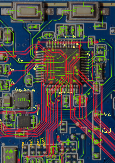
(VDD, GND, PA13/SWDIO, PA14/SWCLK)
Discussions
Become a Hackaday.io Member
Create an account to leave a comment. Already have an account? Log In.