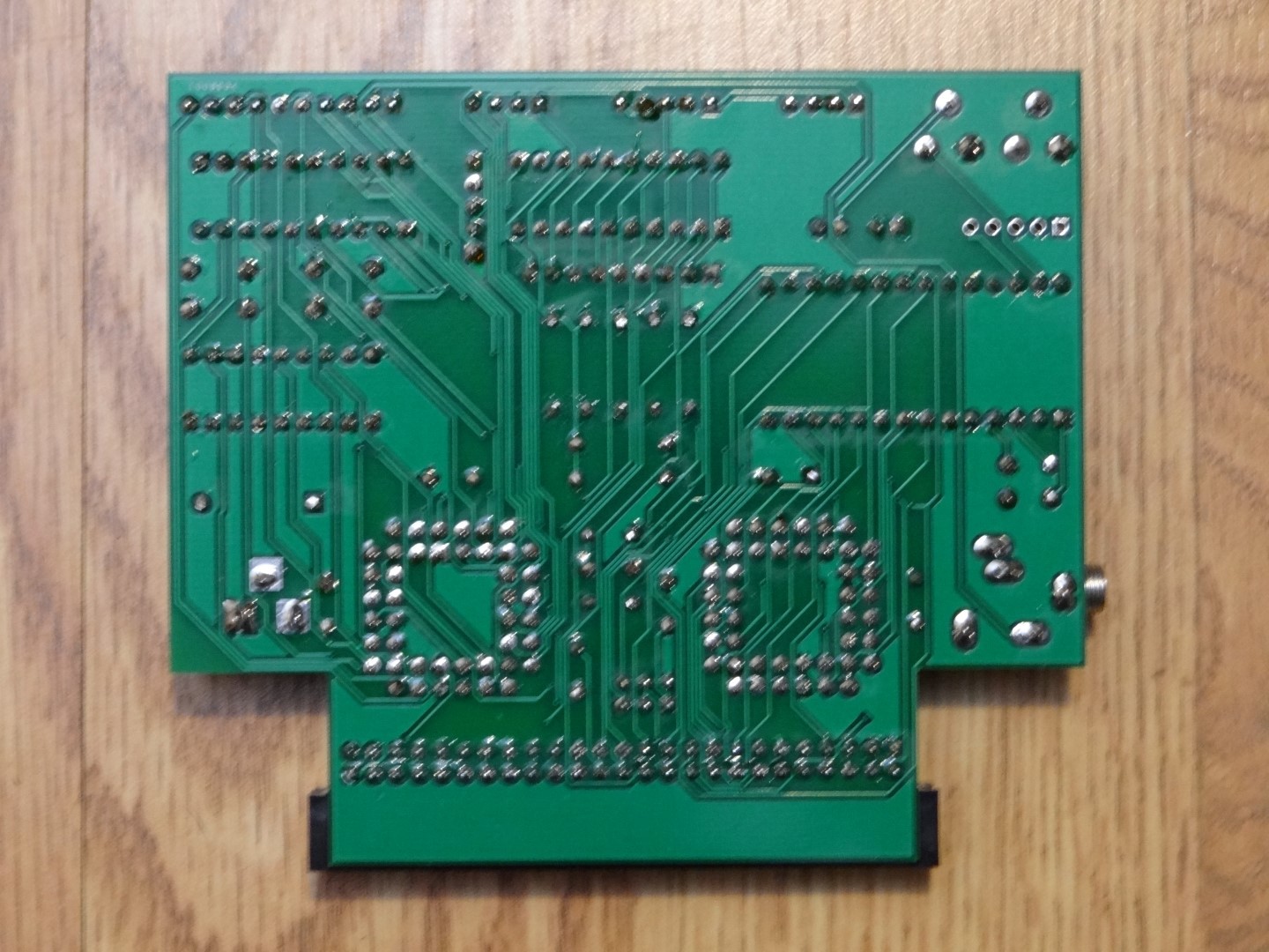
It was bugging me that the previous PCB revision had the SID chip upside down. So I bit the bullet and rearranged the layout a bit. The new PCBs worked out of the box. I also added GND copper fill to the PCB bottom (not sure it makes a difference, but seems to be good PCB design practice). Saifisfied with the PCB now, and declaring the hardware side of this project as done.


 Michael Wessel
Discussions
Become a Hackaday.io Member
Create an account to leave a comment. Already have an account? Log In.