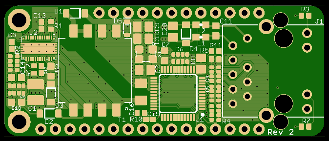
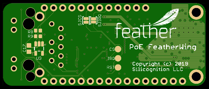
Revision 2 of the PCB layout implements the changes needed to make rev 1 functional, plus some additional goodies:
- Added D5 5.6V zener diode on the PoE output voltage to limit the output voltage under no or low load conditions by providing a minimum load if the voltage goes too high.
- Changed C14 to 4.7uF in 0603 package to make the primary side regulation stable.
- Removed L1 ferrite bead and added C16 and R10 to reset the W5500 on power-up.
- In addition to the default-closed solder jumper that connects the W5500 CS line to pin 22 of the Feather footprint, as present on the Adafruit Ethernet FeatherWing, I also added a default-open solder jumper to connect the W5500 IRQ line to pin 24 of the Feather footprint. This keeps it 100% out-of-the-box compatible with the Adafruit Ethernet FeatherWing, while at the same time making it compatible with the Giant Board without having to run extra wiring, but by just bridging this jumper instead.
- As mentioned before, I had the desire to have a 24AA02E48 on the board to provide a globally unique MAC address since the W5500 doesn't come with one, but I ran out of space for it. I decided to add footprints for this chip plus I2C pull-ups and decoupling cap to the bottom of the board (U3, R8, R9 and C17). Maybe I can produce versions with and without the chip, or maybe I'll just leave them unpopulated so the user can add the parts if desired, or maybe it won't be a problem for the CM to always have it. Either way, it doesn't hurt to have the footprints present while I figure it out. I'd like to get feedback on how useful you think this is in the comments!
- Renamed the solder jumpers SJCS and SJIRQ to make it more clear what's what.
The resulting layout looks like this:


Time to get some boards made!
 Patrick Van Oosterwijck
Discussions
Become a Hackaday.io Member
Create an account to leave a comment. Already have an account? Log In.