megaPanel: A Monochrome LED Matrix Display Panel
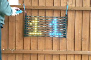
The megaPanel: (16) monochrome LED matrix panels, 8 bits, 120Hz
The megaPanel: (16) monochrome LED matrix panels, 8 bits, 120Hz
To make the experience fit your profile, pick a username and tell us what interests you.
We found and based on your interests.
At this point I have a panel that is free-running, with the exception of one ISR that executes after every row of data is shifted out. But it can only turn the LEDs on or off. There is no shading. This is where things get fun.
At this point, we'd like to use PWM. Simply set the output enable (OE) pin with a PWM value for each pixel when it is being displayed. However, this will not work. Remember from my first project log that each panel displays 2 rows at a time. So if one pixel should have a shading value of 128 out of 256, or 50%, then all the other pixels in both rows will have that shading value as well. Furthermore, since we're using 4 rows of panels and they all share a common OE pin, it would mean that 8 lines on the entire display (128*8=1024pixels) would all have that 50% shading.
Enter BCM. You can get a primer on it here if you are unaware of what it is. But this will not work in its entirety. The whole idea behind BCM is that you would display your LSB for X clock cycles, then display the 2nd LSB for 2*X clock cycles, next for 4*X, next for 8*x, etc,... And X in this case would be the total time it takes to display 1 row, since you can't display a row faster than it takes to write data to it.
Given the above, it would mean that for the 8th bit of shading we would need (128+64+32+16+8+4+2+1) * (1 row display time), which is unacceptable and would crush any chance of having a decent framerate.
To overcome this, we will use a mixture of both PWM and BCM. Here's how it works:
To get an 8-bit depth of shading, we will implement a PWM on the output enable pin of every panel. When we display the first frame, this PWM value will be 1 and will represent the LSB of the byte (8-bits) we want to display. On the next frame the PWM value will be 2, and will represent the 2nd LSB, and so on. On the 8th frame, the PWM will be a value of 128, and will represent the MSB of the byte we want to display.
A side note on the method above: We have to make sure the PWM is completely off before toggling the latch pins in the ISR, else you'll get TONS of ghosting. On the STM32 devices, running in PWM mode, simply setting the capture compare value to zero will not immediately turn off the PWM. This is because the capture compare value is double buffered, and the capture compare register will not update the shadow register until an update event is generated, which under normal timing settings will not happen until an overflow occurs. Therefore we need to not only set the capture compare value to zero, but we also need to force an update event immediately after to prevent the PWM from finishing out its cycle as shown in the code below.
TIM2->CCR1 = 0;		//turn off display
TIM2->EGR |= (1<<0);	//generate update event to force the above into the shadow register and make sure the pwm stops immediately
So we now have Timer 1 controlling the clock and sending requests to the DMA to transfer all our data, and we have Timer 2 controlling the PWM for the OE.
The above method allows us to create 8 bit (or whatever you choose) shading, using PWM and BCM, all in 8 frames of the display. Moving forward, when I calculate framerate, I'll divide the actual framerate by the bit depth (8), since 8 frames represent a full frame.
Most people say to run 100FPS minimum for LEDs, so your microchip should actually be refreshing the screen 100*8=800 times per second to achieve a fluid look.
As a side note on this, to my eyes, an FPS of 80 is adequate and sufficient until you try to take a photo of it to share with the community. For this, a framerate of 150+ FPS is desirable. At the time of writing this, my panel is running at 300FPS with 12-bit shading, meaning it's actually refreshing 300*12 = 3,600 times per second. <--And I still have more horsepower under the hood! Bless you, STM.
Have you ever cleaned your workshop, only to find that nothing can then be found? In it's prior state, it may be messy, but you know where everything is. Unfortunately, this is the case for the buffer that is sent out via DMA.
So you have a bunch of data that you want to display on the screen. And it's in a logical order. It's likely in a format that reads left to right, top to bottom. Now, you have a crazy thing called 'DMA,' who's contantly throwing data from the buffer at the panel, in a format that the panel can understand. If we were to keep things neat, and use the logical left to right, top to bottom insertion of the data into the buffer, you'd find that your data is NOT where you want it to be on the physical screen.
You have to know how these panels are scanned. These particular panels scan from right to left 8 bits, then jump down 4 rows, scan right to left another 8 bits, filling 4 rows before returning to the top to scan another 8 bits before jumping down to the next row. I'm sure it's intelligent design for some special controller out there, but I find it obfuscated.
Rather than create logic rules to define where the appropriate pixels are to be inserted into the buffer (believe me, I did this in OpenOffice Calc, and it's not pretty) I opted to use a lookup table, or LUT. The LUT is an array of 128*64*2bytes=16,384 bytes that defines the location of the pixel in the buffer based on the address of the variable in the array.
But wait, since the scanning is the same for all panel chains (remember there are 8 sets of 2 panels chained together), we can create 1 LUT that is common for all the individual panel chains, rather than the entire display to save memory. The resulting LUT would therefore be 16*64*2 = 2Kb, where 16 is my Y axis of one set of (2) panels, 64 is my X axis of two panels side by side, and 2bytes (16-bits) are needed to store the location since the value of their locations can go over 255.
The above picture is generated via formula in Calc, in which I exported to CSV to extract the data in a format that can easily be pasted into a complier. So for instance, if you want to turn on the 3rd pixel from the top left, using the LUT array, you could get it's position in the buffer by position=pixelLUT[0][3]; This will return the value 997, where 0 represents the first row, and 3 represents the 3rd pixel from the left.
void placepixel(uint8_t xpos, uint8_t ypos, uint8_t pixeldata, _Bool gammaOn){
	if(gammaOn){
		pixeldata = gammaCorrection[pixeldata];
	}
	//what panel and pixel are we addressing?
	uint8_t ypanel = ypos / 16; //should return 0 to 3
	uint8_t xpanelpos = xpos % 64; //should return 0 to 63
	uint8_t ypanelpos = ypos % 16; //should reutrn 0 to 15

	//Determine what bit position to place the bits, this is dictated by what panel section is connected to what port # on portB
	uint8_t bittoplace = 3 - ypanel;
	if(xpos > 63) bittoplace += 4;

	//set the pixel in the buffer (0=on, 1=off)
	uint16_t bufferposition = pixelLUT[ypanelpos][xpanelpos];
	//pixeldata = ~(pixeldata);

	for(uint8_t ibcm=0;ibcm<8; ibcm++){
		panelBuffer[(bufferposition + (ibcm*1024))] |= (1<<bittoplace);			//clear the bit in position
		if(pixeldata & (1<<ibcm)){												//if the pixel needs to be on
			panelBuffer[(bufferposition + (ibcm*1024))] &= ~(1<<bittoplace);	//turn pixel on
		}
	}

}
The above is the code I use to insert pixel data inside of the free-running DMA buffer. It is a function that will take an absolute X Y value, determine what set of panels we are addressing (there are 8 sets of 2), then use the LUT, combined with the panel pair information to determine where to insert the data.
I haven't written about this yet, but the ibcm is for bit coded modulation. I'll get into that at a later date, but for the purposes of trying to understand the above code, for every bit depth of brightness on the panel, the buffer size is (128*64)/8=1024 bytes. Remember that these are not color panels,...
Read more »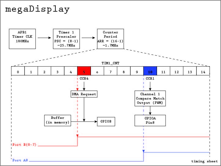
Please study the goodness that is the above image. The display driver I wrote is free-running, constantly outputting the contents of a buffer in memory to the GPIOB port via DMA while taking care of the clock pulses using the same timer via PWM. The trick here is to sent the DMA request prior to the CCR1 compare match (and therefore clock signal high).
The red & blue lines represent the signal on the GPIO pins as if they were viewed on an oscilliscope. As you can see, at an approximate 1.7Mbps, we'll be able to achieve a solid framerate. Besides, we'll need those extra frames if we want any sort of bit depth.
So we've setup timer1 with a 15 count period, setup TIM1 Channel 4 to request a DMA transfer at compare match with CCR4, setup TIM1 Channel 1 to output a PWM, using CCR1 as a compare match. Note the PWM is in 'LOW' mode, meaning it stays low until it experiences a compare/match with CCR1, then goes high.
"But how do we handle row switching,?" you may ask. This is where ISRs come into play. We basically count the number of overflow events (timer CNT reaches ARR, then resets back to zero), so we know how many pixels we've shifted out. Once we have shifted the last pixel in the row, we stop the timer, toggle the latch and OE pin, set the pins to the appropriate row on the GPIO port, then again toggle the latch and OE pin to latch the data and enable the output. We then start the timer to repeat the sequence.
But wait, it's not that easy. ISRs take time. With a clock running THIS fast, by the time we enter an ISR routine in software and disable the timer, we may get ~1-4 extra clock pulses for each row. This clearly won't work in its current state.
The solution is to use two different Timer tools at our disposal. The first is the repetition counter (RCR) and the second is one pulse mode (OPM).
The repetition counter is a register that will count down at every overflow event on the timer it is setup for. When the repetition counter reaches 0, and only when it is at 0, is when an overflow will trigger an ISR AND an update event will be generated. It is important to note that an update event will not be generated on timer overflow until the timer overflows WHILE the RCR is at 0x0.
With this, we set the repetition counter to 255. Remember you need an overflow while RCR is 0, so zero is counted, and 256 pulses will output before the ISR is triggered and the update generation event occurs. The update generation event is automatic, and reloads the contents of the ARR, CCRx, RCR, etc into the shadow registers -- this is because they are double buffered in this mode.
So this allows our ISR in software to not be triggered until an entire row has been shifted out. This is great, as it's one less thing we have to keep track of in code, and it is automatic. But how do we stop the clock to prevent extra pulses from getting in? Remember the timer is still counting when we enter the ISR, and if you're not fast enough (and you likely won't be at this speed) then your data will start spewing into rows it should not be.
Enter the OPM. One pulse mode stops the timer at the next update event. This is great in that now our timer is stopped via hardware immediately after the row has shifted out (remember we're not generating update events until RCR=0, and therefore not until the entire row has been completed). This leaves our ISR in software to only have to worry about toggling the OE & LAT pins, selecting the next row via the LED Display's A & B pins, re-toggling the OE & LAT pins, then restarting the timer.
The board I'll be using to drive the megaDisplay is a Nucleo-F446RE, which sports a STM32F446RE chip, operating at a maximum speed of 180mHz, with 512 Kbytes of Flash memory and 128Kbytes of SRAM. Since I'll be sharing the A, B, OE, Latch, & Clock pins for each board, I'll need a total of (8 DR, 1 LAT, 1 CLK, 1 OE, 1 A, & 1B) 13 pins going to the Nucleo.
In an attempt to keep things tidy, I've opted to create a quick & crude PCB to accept all the inputs to the panels. I could have ordered a PCB to keep things neater, but this was the quickest solution. Many jumpers abound.
After quickly adding pin headers in Eagle, I compiled the board layout below
Then it was out to the garage to mill it on the CNC.
The jumpers were a temporary solution until the female pin headers I ordered came in. The Bx numbers represent the port numbers on the STM32F446RE, which each panel will have its own specific DR pin for the transmission of the display data. Note B0-B7 were used since it's been decided to use DMA for the data transfers.
The final board can be seen below with all the jumpers, female pin headers, and Nucleo board installed.
Since I'm using a STM32F446RE to drive this panel, I'll be driving the data pins (DR) using DMA on the STM32 chip.
The way this will work is the DMA controller will receive a request from a peripheral. Once the request is received it will copy a byte from an address in memory to another address in memory. I'll go into specifics later, but we will be copying an array in memory to the GPIO pins to spew out our data. The request will come from a timer, which will also act as the clock signal for the panels.
The DMA controller can either copy a byte (8 bits) or half word (16 bits) to the GPIO pins. Looking at the panel layout sheet below, you can see I have chosen to daisy chain the left (2) panel rows together, and daisy chain the right (2) panels together.
The lines and arrows represent the data into the panels, and you can see that I'll be using 8 data lines (DR pin) to drive the megaDisplay.
Since I'm making use of the DMA feature to automatically change the states of the data pins, I could technically use the DMA to transfer half word to the GPIO port, or 16 bits at a time, allowing me to drive each panel's (since there are 16) DR pins individually. In this case, none of the panels would be linked together. This would allow for the fastest framerate given my hardware, but has the downside of requiring more wires and connections to the boards.
I could have very well chosen to daisy chain each row together, allowing the need for only (4) data lines in, but the framerate would suffer. One byte, or 8-bits, is a great tradeoff, requiring only 8 data pins in (DR pin), makes use of DMA's one byte transfer, and is a happy medium for achieving a good framerate.
While I haven't begun programming yet, the sequence would look something like this:
Each panel has the following PINs:
OE, GND, A, B, CLK, LAT, DR
OE is output enable, and it is active HIGH, meaning when the OE pin goes high, the LED panels are illuminated. This pin can be fed a PWM signal to adjust the brightness of the display, but it would have to be carefully timed to prevent ghosting. More on this later.
Pins A & B select the row that is to be displayed. Given (2) bits, A & B pins, there are a combination of 4 different values that can be given to these panels. This is a tip off that the mode of these panels are 1/4 scan. Since each panel is 32 pixels wide by 16 pixels tall, this makes for a total of 512 LEDs per panel. 512 divided by 4 rows equals 128. This indicates we'll need to shift in data in 4 segments, each time shifting out 128 bits. Since there is only (1) DR pin for data, we know we'll be shifting out 4 rows (128 bits divided by 32 pixels) at at time.
CLK is self explanatory. When the CLK pin goes high, the bit that is present on the DR pin gets shifted into the register. This means we'll have to change the state of the DR pin prior to the CLK pulse.
LAT is the latch pin.
DR is the data that gets shifted into the registers on CLK high signal, and it is active LOW, meaning when the data is shifted in, the corresponding bit lights up the corresponding LED when the DR pin is LOW. This is a bit backwards from what I'm used to (active high on HUB 75 panels) but not a major issue.
The driving sequence then for each panel is as follows: (initial startup with OE pin high and LAT low)
My initial thinking is that I can use shared pins between the panels. For instance, tie all the CLK, LAT, OE, A, & B pins together. My only concern with this is signal capacitance on the lines and the fan out capability on the MCU, which I won't worry about for the moment. I'll just move forward until something goes wrong, then assess the problems.
Given this, the entire display of (16) panels may theoretically be ran off of 6 pins, not including GND. I will, however, be using 13 pins for this setup which I will explain at a later time, when I discuss the driving method.
My original thought was to use a piece of plywood, but I opted for a frame for the following reasons:
I did a quick sketchup model of the frame, just to verify dimensions.
I opted for poplar, because the pine at my local home improvement store was too warped and knotty. I purchased a couple 1x6x6' poplar boards, and ripped them down to 2.25" on the table saw, so I could get 2 rips out of one board.
After cutting the boards to length, I used a mini Kreg pocket jig to assemble the frame, while putting a dab of wood glue between each joint.
And the completed frame...
The frame ended up being extremely light and straight, and will still allow access to the backs of each LED matrix. You can see a couple of the Matrix panels in the background, which I was using for testing.
Next step is to mount the panels to the frame. For that I needed to order some M4x.7x25mm screws. 25mm allows each of the screws to stick out of the frame ~1/4", since the 1x boards were 3/4"
Each of the panels has (4) threaded receivers for screws. Rather than measure for each hole and risk having gaps in the panels or the screw holes not lining up correctly, I opted to create a template of the panel with the screw holes shown below.
In this way I could mount the upper left panel on the corner, then butt the template up to the mounted panel, and finally drill for the next panel. Below you can see the assembly after mounting the first 6 panels.
Unfotunatley, I'll have to wait to complete the install of the LED panels, as I'm waiting for more screws to arrive in the mail. The local hardware stores only sell the metric screws by the single, so at 64 screws, the cost would have been too great to purchase locally.
I just got off a 2 week project where I tasked myself with driving a RGB matrix display, HUB 75, P4, 64 x 32 pixels. I had an extremely great time learning and programming it, and it was my first introduction into the line of STM32 boards and ARM processors. Naturally, I wanted to go bigger, but I was only able to achieve a framerate of 45hz at a color depth of 24 bit, this with a 72mhz STMF103C8. The results were outstanding. After completion of this project, I realized more efficient ways of using this chip, as well as some hardware features that could be utilized to increase the framerate. On testing of this panel, I was using BMP files to display images that were resized to 64 x 32. One of the images I uploaded to the chip was a grayscale image of a cat. It looked fantastic, and I decided I could scale the project up with all white LED panels, since the lower drive requirements of switching from color to monochrome would alow me to drive a larger panel, or series of panels while maintaining a decent non-flicker framerate. I'm shooting for a minimum of 100hz refresh on this display.
Create an account to leave a comment. Already have an account? Log In.
Become a member to follow this project and never miss any updates
 ccates
 LordGuilly
Hi George Gardner, very nice work and informative project logs.
can you please share the code. i would like to learn pwm and grayscaling.