By BP:
Routing
It’s been a long time since the last post. I’ve been busy finished the routing of our vertical PCB. We use 4 layers, layer 2 being a GND plane.
Here is the routing layer by layer, with explanations:


FPGA architecture
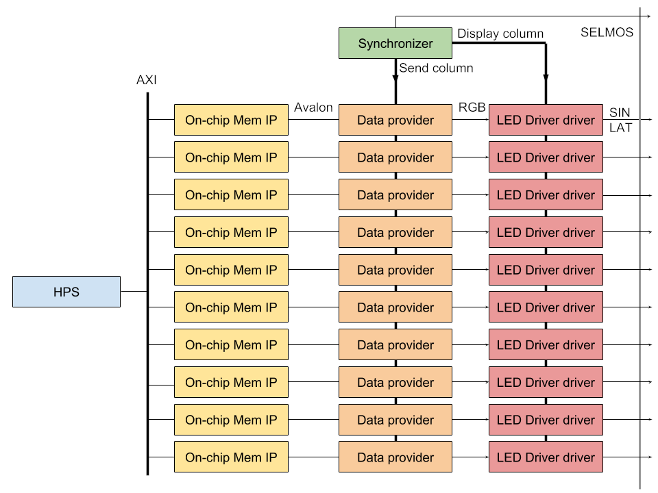
Since we’re done (modulo reviewing) with the PCB, we started thinking about the FPGA architecture.
We came up with an architecture based on 4 modules.
- We will use the Altera On-chip Memory IP as our per-driver buffers. It is practical since it has an AXI-compatible interface that we can use to easily connect to the HPS.
- A synchronizer module will be in charge of time-keeping in order to load and display data at the right time. It will also select which column to display.
- The data provider will load data from the memory and pass them to the LED-driver driver.
- Finally, the LED-driver driver is in charge of creating the SIN/LAT signals. It will both send data to the driver (as requested per the data provider), and display those data (as requested per the synchronizer)

 Alexis
Discussions
Become a Hackaday.io Member
Create an account to leave a comment. Already have an account? Log In.