 MagicWolfi
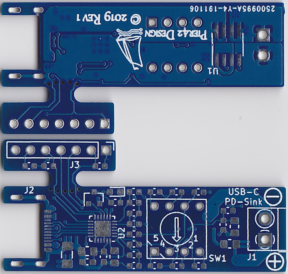
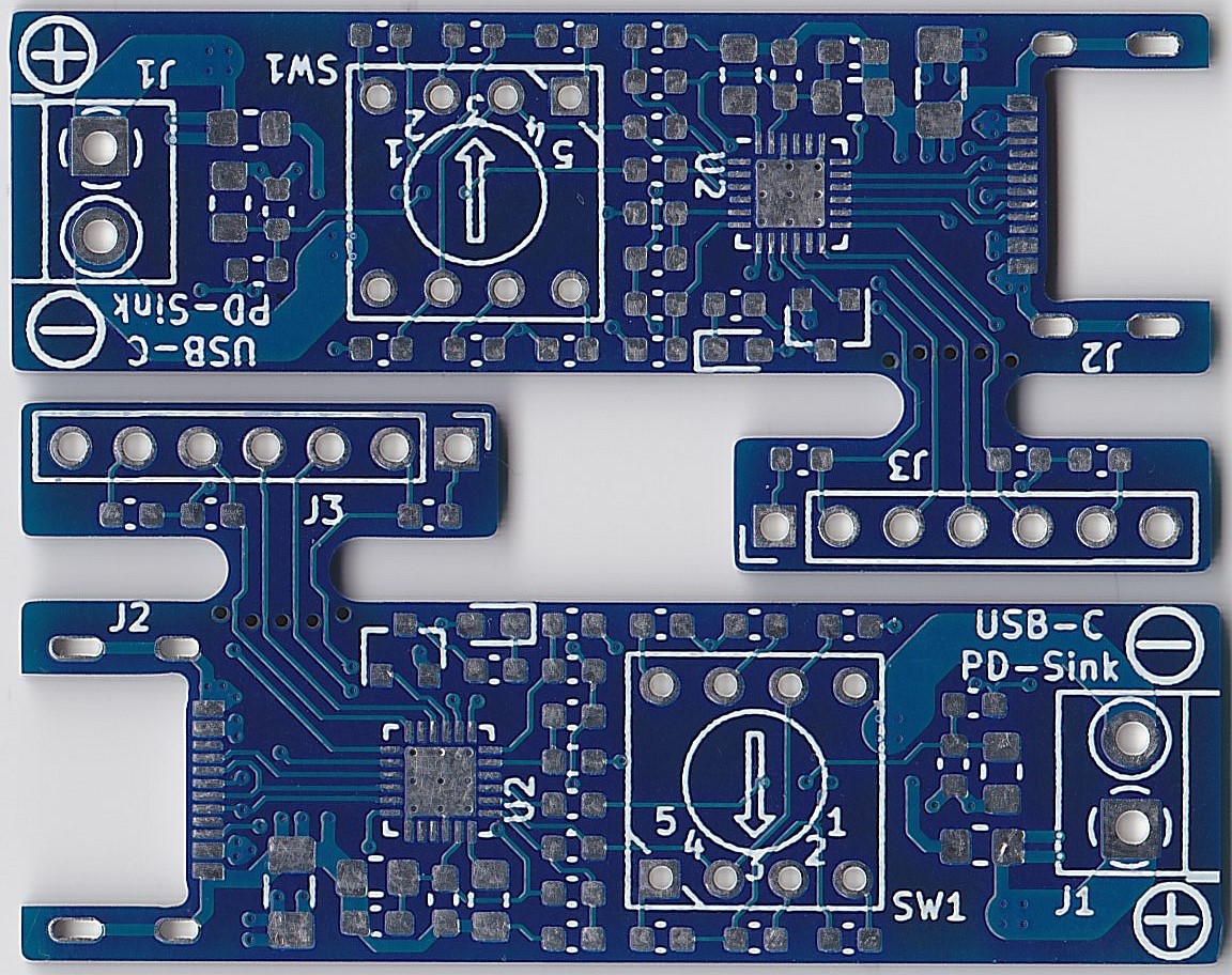
The PCBs arrived from JLC. Optical inspection is a pass and I can clearly see the thicker traces with this 2oz copper layer design. I'll do some testing first before I am going to test the break-off tab feature.
All components are here also, so I am off to the workbench.
Discussions
Become a Hackaday.io Member
Create an account to leave a comment. Already have an account? Log In.