 David Knochenhauer
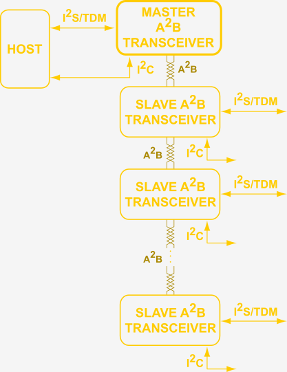
What is A²B?
From ADI product website:
A2B is a high bandwidth, bidirectional, digital audio bus. A2B is capable of transporting I2S/TDM/PDM data and I2C control information, along with clock and power, using a single, 2-wire UTP cable over distances up to 15 m between nodes and 40 m over the entire daisy chain. A2B can be used as its own network with embedded sub-networks, or as an endpoint transport bus used in combination with other, longer distance protocols. The clock is synchronous on all nodes in a single A2B network. Microphone and serial audio data is received on each node in the system simultaneously.
High bandwidth, bidirectional, digital audio bus
The bandwidth allows up to 32 upstream and 32 downstream channels, depending on resolution. The bus runs with 1024 times the sampling frequency.
 Source: ADI AD2428W Datasheet
I2S, TDM, PDM, I2C
One can imagine A²B as a prolongation of the normally PCB-bound (Inter-IC) interfaces.
This interfaces can be fed into one A2B node and pulled out of others.
- I2S (Inter-IC Sound)
- 3 lines (serial clock, word select, serial data)
- one or two channels (mono, stereo)
- Single Master, multiple slaves
- TDM (Time Division Multiplexing)
- similar to I2S but allows up to 16 channels of data
- rather than indicating left or right channel by 50% duty cycle clock, the TDM frame is indicated by single bit pulse
- PDM (Pulse Density Modulation)
- 2 lines (data input, clock)
- single direction
- often used by digital MEMS microphones
- 2 channels per por
- I2C (Inter-IC Control)
- 2 lines (serial data, serial clock)
- multi-master, multi-slave
- bidirectional
- 400kHz or 800Khz
Clock, Power, Cable
All nodes have their own PLL, which derives the clock from the Master clock. The Master get's his clock by the host system and is normally the audio sampling clock (44.1kHz or 48kHz). Since all nodes run on the same clock they are all synchronous.
A2B is able to provide phantom power. Each locally powered node can provide up to 2.7W (9V,300mA) to downstream nodes.
The Cable needs to be an unshielded twisted pair wire such as standard network cables (<Cat. 5e). One can extend the bus to 10 slave-nodes with up to 15m cable between each node (40m over the entire chain). Each node has 2 ports and 2 transceivers connecting it to the neighbor nodes.
Extra Features
Each node has several GPIO pins which may have alternate functions.
- IO0-IO7
- can be used as digital output or input with interrupt capability
- each pin can be mirrored to the master node by using the "GPIO over distance" feature
- DTX0/1,DRX0/1
- two I2S/TDM interfaces per node
- PDM
- The DRX pins can be used as PDM Interfaces
- up to 4 PDM microphones per node
- internal LDOs
- providing 3.3V and 1.9V to the transceiver and peripherals
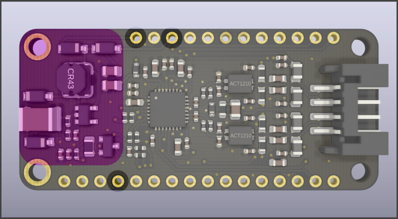
The A²B Feather Wing
Since A2B makes the most sense when I2S is used, the wing was designed with Feather M0, Feather M4 or STM32F405 boards in mind. Other boards are still able to control the bus via I2C.
Overview
- AD2428W A2B transceiver
- Master capable
- up to 10 nodes
- A+B TRX blocks
- I2S/TDM support
- up to 4 PDM mic
- 9V Boost converter
- boosts feather 3.3V to A²B bus compatible 9V (for max. phantom power)
- LT1930 convert
- EMC circuitry
- Everything from ADI's circuit recommendations implemented (beside a notch filter for AM bands)
- JST Series PH connector
- The connector adafruits loves and uses for their STEMMA connections. Just need to twist the wires and repin the housings
- Jumper Options for I2S routing
- on the bottom side you can modify routing for your feather board
Pinning
Power
As the phantom Power of the Bus is 9V there is the need for a boost converter (purple area). Logic voltages for the A²B Transceiver are generated locally by internal LDOs of the transceiver and thus it makes sense to not use the Feather's 3.3V supply but VBus or VBat.
The A²B Wing is powered from Bat or USB and connected to Gnd (of course).
Serial Data Pins
The A²B Transceiver is configured using the I²C Interface via Pins SCL and SDA.
The default connections fit for Feather M4 or ST32 boards where you have a fully fledged I2S Bus.
See the next chapter for M0 configuration.
For Master operation a clock is required which is derived from the Word Select (WS) aka SYNC signal from the I2S Interface. By default it is connected to pin 10 (I2SFS0).
I2S Data is connected to pins 12 (SDI) and 11 (SDO).
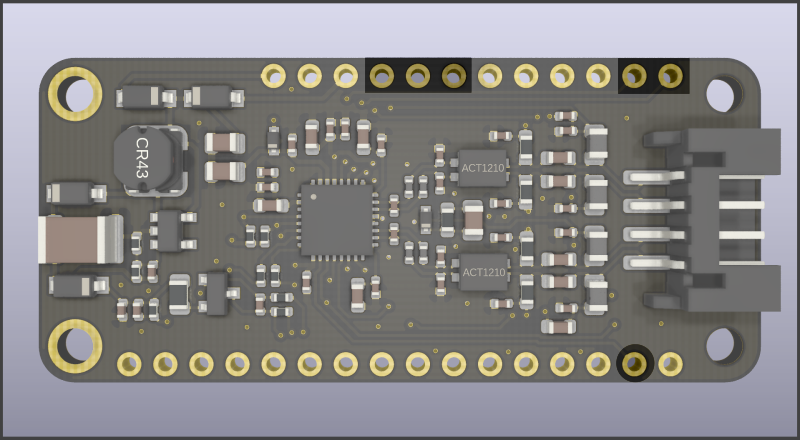
I2S Clock (BCLK, I2SCK) is connected to Pin1 (TX) in the lower right.
Optional configuration for Feather M0
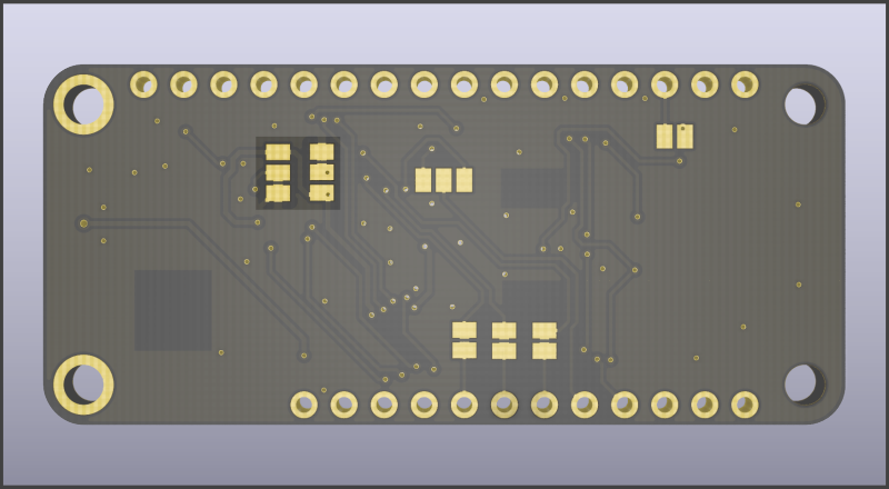
On the back of the board you find five solder bridges for optional I2S routings.
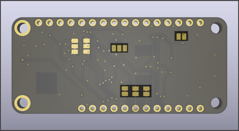
On the lower side you can disconnect the default lines (SDI, SDO, WS) from above mentioned Feather pins. You can leave the pins connected as well and use them as GPIO pins.
One can then router either SDA (DTX1 at AD2428) or SDO (DRX1 at AD2428) to pin D9 of feather. That pin is used for I2S/Data on Feather M0 boards. In the top right you can connect the WS (SYNC) signal to pin D0/Rx of Feather. That pin is also used for I2S/WS on Feather M0.
Bitclock stays at pin D1.
GPIO
All I2S pins can also be used as GPIO pins if configured correctly in the A²B Transceiver AD2428W (and at the Feather of course). Additionally pin D6 is connected to IQ0/IRQ pin of AD2428W, which can be used as a GPIO or Interrupt from this chip.
I2C Address
Due to the nature of the A²B Transceivers each node has two I²C Addresses, one to access the registers of the connected transceiver (BASE_ADDR) and one to access the registers at other nodes on the bus or even of peripherals attached to other nodes on the bus (BUS_ADDR).
| ADR2/IO2 | ADR1/IO1 | BASE_ADDR | BUS_ADDR |
| 0 | 0 | 0x68* | 0x69* |
| 0 | 1 | 0x6A | 0x6B |
| 1 | 0 | 0x6C | 0x6D |
| 1 | 1 | 0x6E | 0x6F |
7-bit Addresses without the R/W bit, *default address
A pullup/-down resistor is already in series so you just need to break/solder the appropriate traces.
Glossary
| Term | Explanation |
| upstream | Everything that goes "upwards" towards the Master node |
| downstream | Everything that goes "downwards" towards the last slave node |
| A-Port | The Port that points upstream, towards the Master |
| B-Port | The Port that points downstream, towards the last slave. |