 michal777
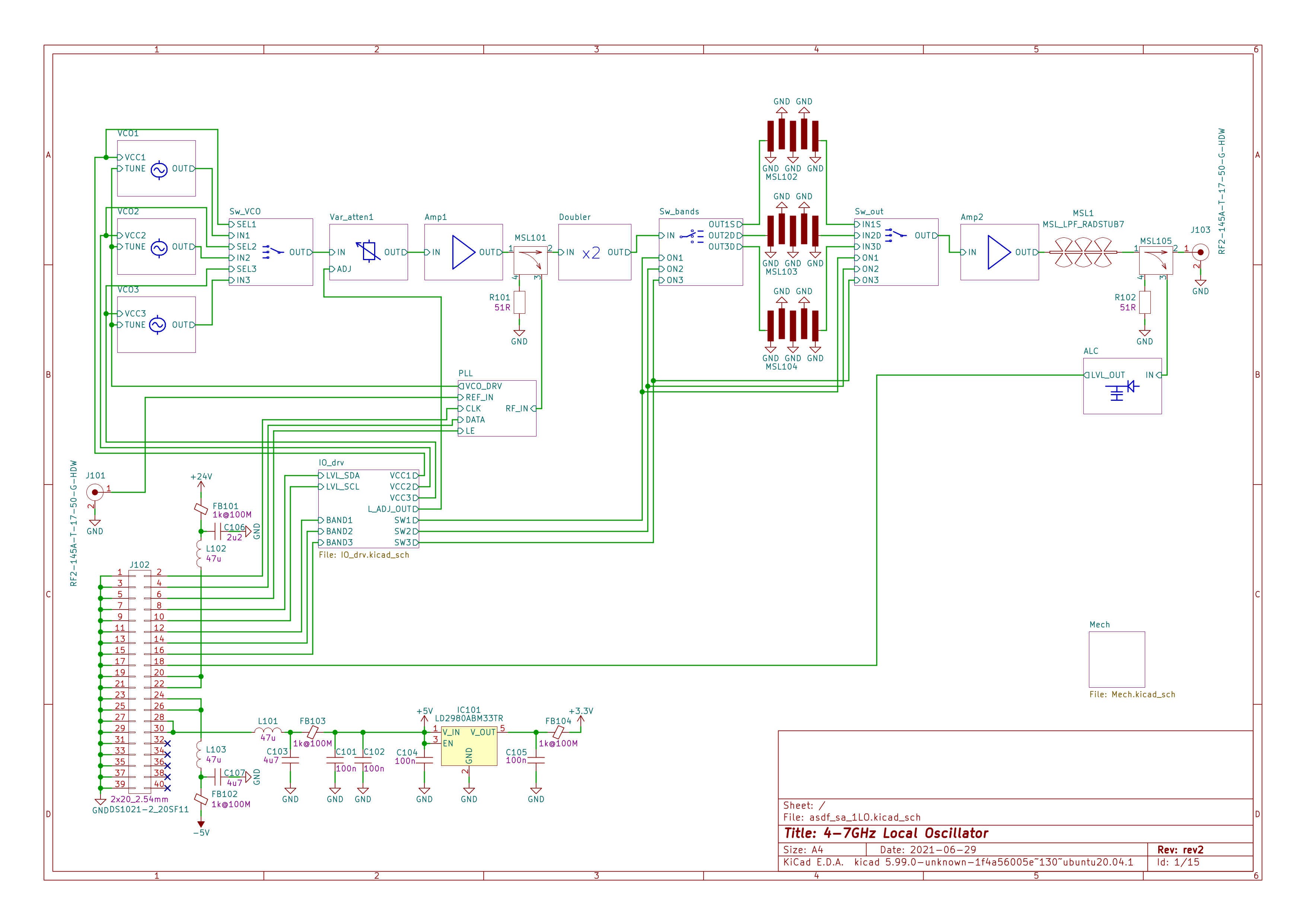
I've made a new revision of the project. See LO1rev2_design_pack.zip for KiCad design, various simulations, design description. It's mostly redesigned, a little simplified although still I didn't try to avoid silly design decisions so don't expect high performance or usefulness of the design.
Short summary of changes:
- In general, more components are wideband, previously there were mostly three signal paths for each sub-band (4-5, 5-6, 6-7GHz)
- VCOs - Changed to a normal Clapp oscillator, I had some problems with this topology in 1st revision but it seems to be working OK if parasitics are reduced (tight layout, only single tuning diode). It works (that's all I can tell about it's quality).
- Attenuator for gain control - Simple 4 diodes attenuator IC. It's simpler and works better because it's wideband (previously three circuits with distributed elements).
- Amplifiers - 2-3.5GHz and 4-7GHz amplifiers are similar. I used some resistive matching to avoid bad SWR which was a problem in previous design. In my previous design lossless components were used for matching so in order to reduce gain at lower frequency (to get flat gain over frequency) a lot of power had to be reflected. In the rev2 design the power at lower frequencies is mostly dissipated in resistors (kind of a simple non-reflection filter at the input). I had too much gain before frequency doubler so I added attenuator and not enough gain after the doubler so I've cut a hole in PCB and inserted 4th gain block.
- Frequency doubler - It's a wideband doubler, based on marchand balun. It was quite a fun to make an useful balun on poor man's substrate, this part mostly forced substrate thickness for the whole design. Details in documentation. Insertion loss is about 10-15dB which is sufficiently good for me, considering simplicity and price.
- Switches for filters - The first design in rev2 was very good in simulations but totally useless in real life (parasitics...). I made a simpler switches to reduce insertion losses (cut the old from PCB and replaced with a new one on self made PCB). The best solution would be to use a real, integrated circuit switch instead of building it from diodes (7GHz is too much).
- Filters - Only small adjustments, mostly the same as rev1.
- Added low pass filter at the output - not sure if it helps or not (may be even harmful because of high losses @7GHz, @FR-4
- PLL and ALC similar to rev1.
Unfortunately I've not much possibilities of measurements above 6GHz (up to 6GHz I use arinst-ssa, although it has undefined performance above 3GHz), also measurements in the circuit (without cutting out a measured block or making a new copy) are inaccurate (SWR of connections matters a lot) so I'm highly uncertain about performance of particular circuits. The whole synthesizer provides about 7dBm max over the 4-7GHz range, if I can trust a 20$ power meter (I can't actually...).
Discussions
Become a Hackaday.io Member
Create an account to leave a comment. Already have an account? Log In.