 michal777
Method of testing
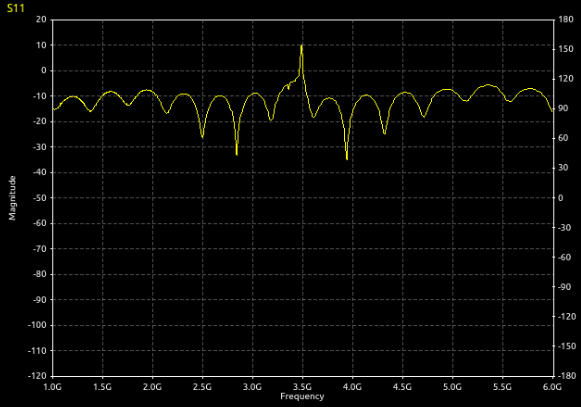
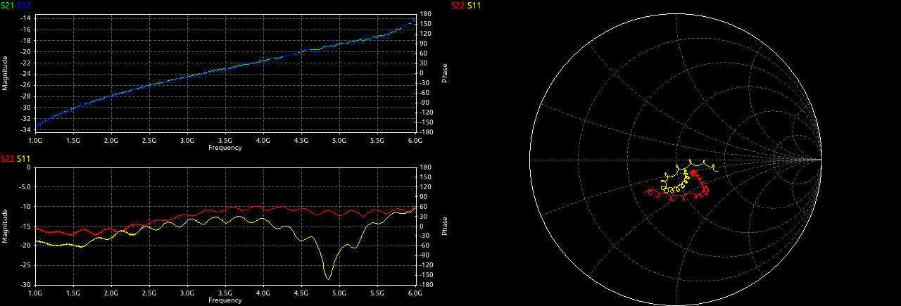
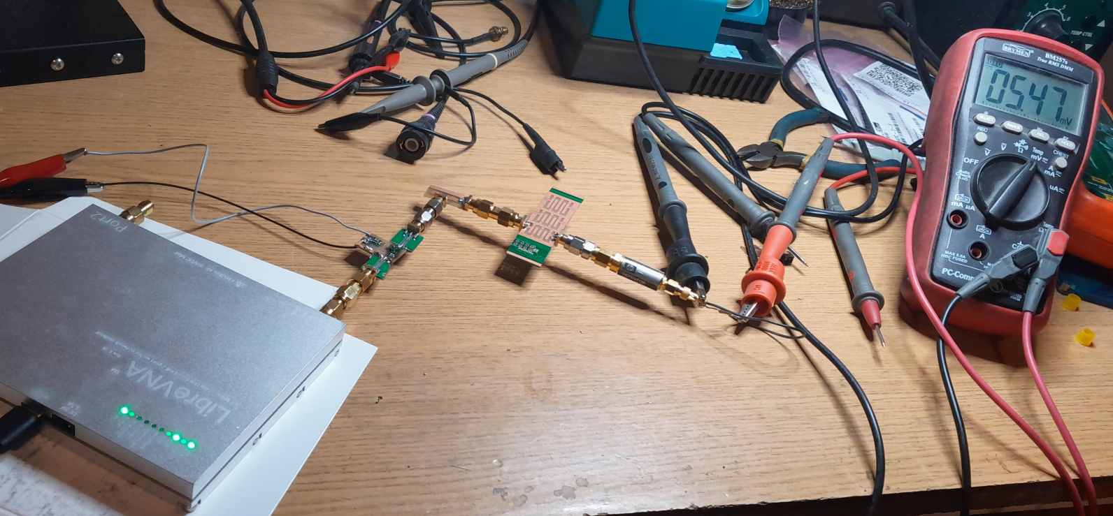
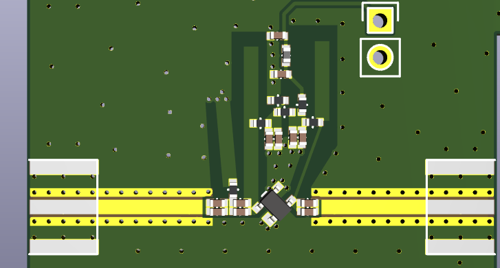
Most of measurements are done using librevna. It has harmonic mixing mode which allows to make some measurements above 6GHz (although be careful with measurements of active devices and fundamental frequency is still there). Calibration was done using PCB test fixtures as shown below (SOLT or TRL possible).
VCO
One of the VCOs was tested – 3-3.5GHz. Output level was tested with LibreVNA, previously calibrated using good RF generator. The level is near to 0dBm in the whole frequency range. The results look ugly because 1. LibreVNA is not spectrum analyzer and shows the unwanted tones, 2. no shielding, 3. no closed loop PLL, just VCO alone so the low frequency noise is not filtered by PLL.
Example measurement:
VCO 3-3.5GHz, at 3GHz, 50R added in series, measured value with added
10dB attenuator - power -1.5dBm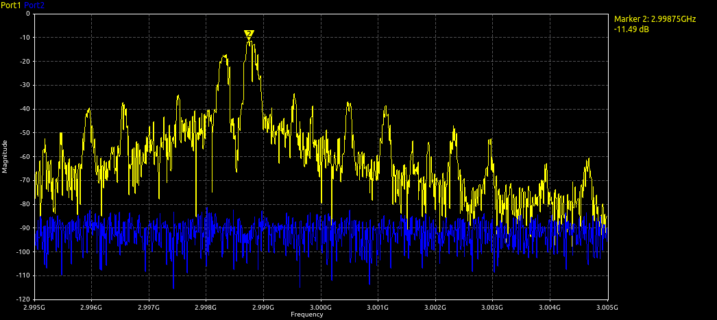
VCO selection switch
Not tested but expected to be not worse than filters switch
Variable attenuator
Typical application of BAP64Q 4-diode attenuator – 2.7dB insertion loss, 23dB attenuation at 3.5GHz.
 Full on:
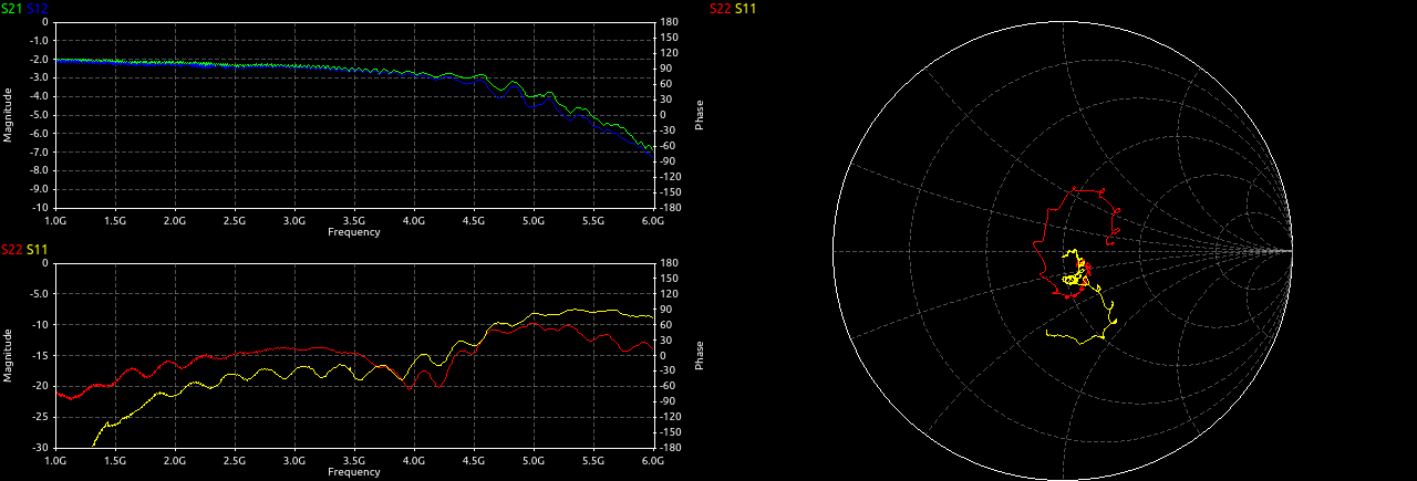
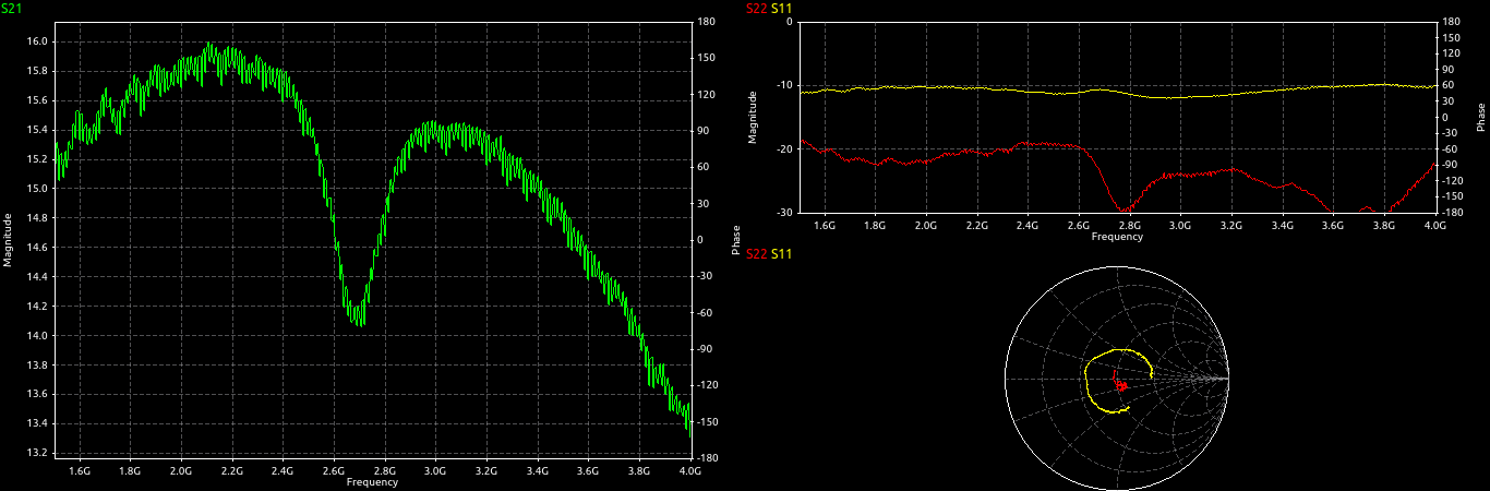
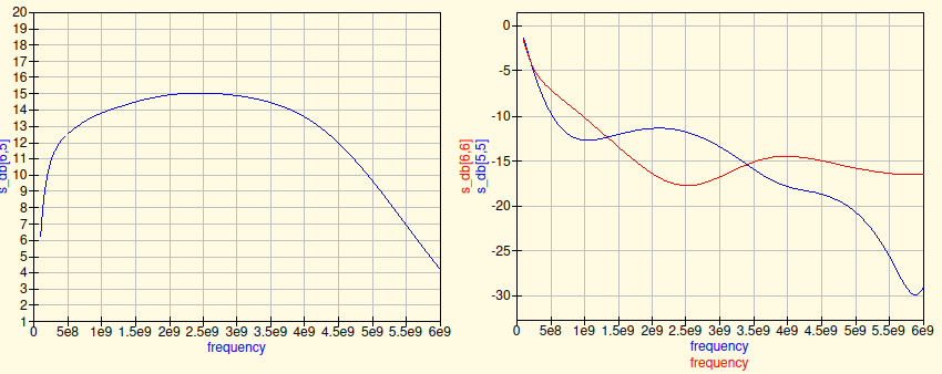
2-3.5GHz amplifier
Initially there was
a weird shape of gain characteristic.
Doubler
It’s hard to test because I’ve no proper equipment for the task. I tried testing is in connection with amplifier to drive it with reasonable level and output filter to have only one tone – then the signal is measured with a HP 33330B detector. Power of the signal with amplifier is compared with power of the signal after doubler and filter.
Loss of the doubler is probably about 10dB (13-16dB including with filter)
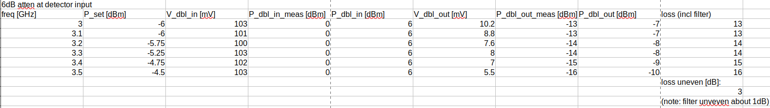
Also I did simulation in spice which confirms about 10dB loss and confirms that doubling works best with not too high input power, less than 10dBm.
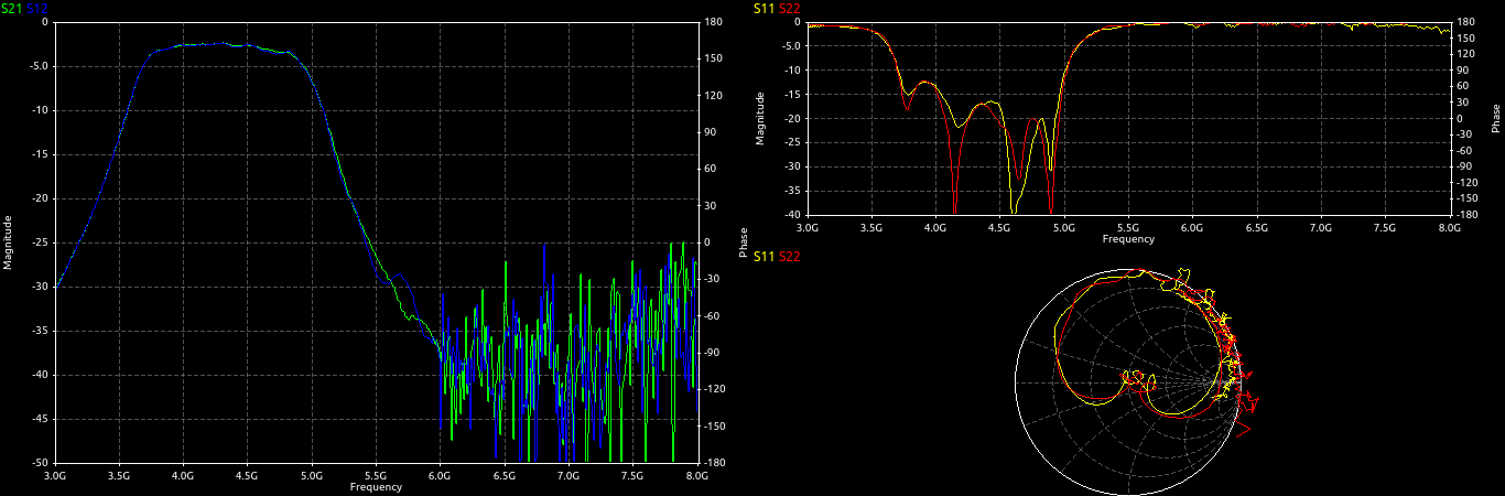
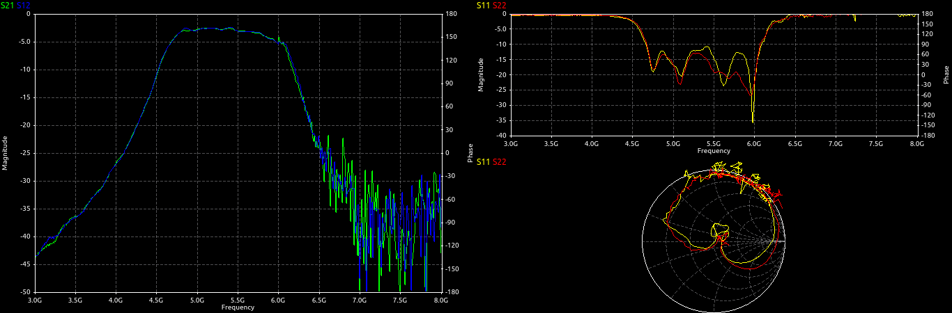
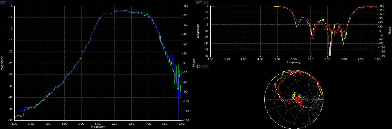
Filters
Filters were measured and the results were ok, loss better than 5dB on FR4, only center frequencies should be slightly increased.
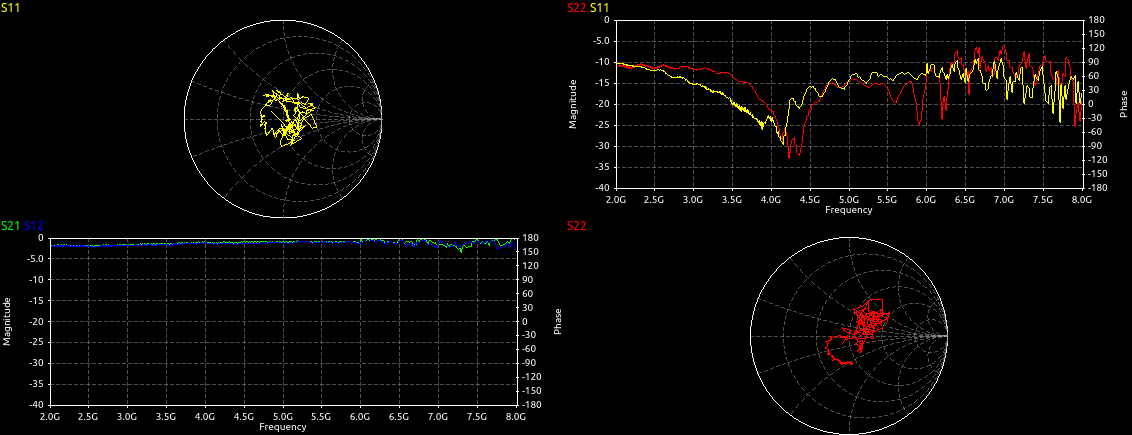
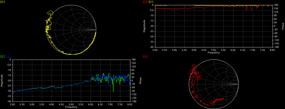
Switches for filters
Only one diode
tested. The switch was redesigned. Two PIN diodes in series provides
better attenuation when off and have not bad insertion loss when on.
Larger pieces of copper between the diodes are to partially
compensate diodes inductances by adding some capacitance (works in simulation, not sure if also
in real world).
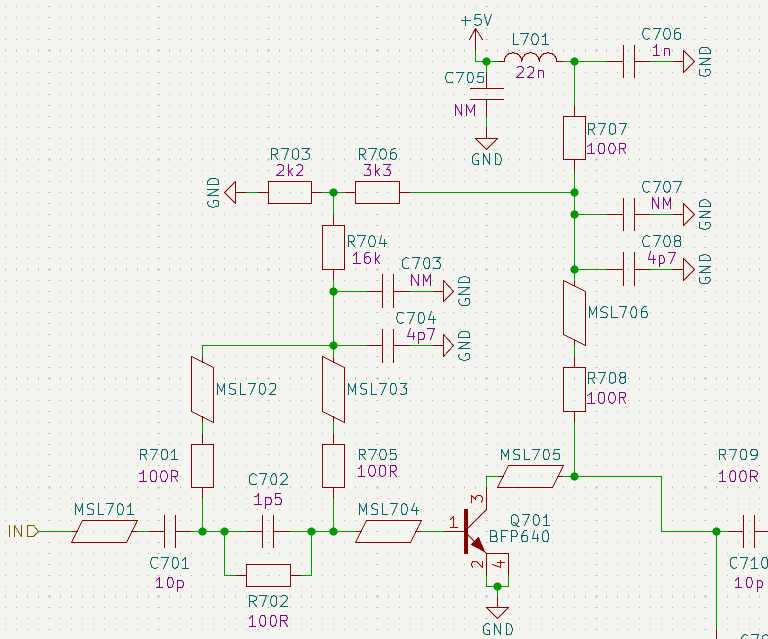
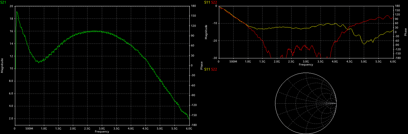
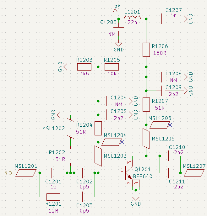
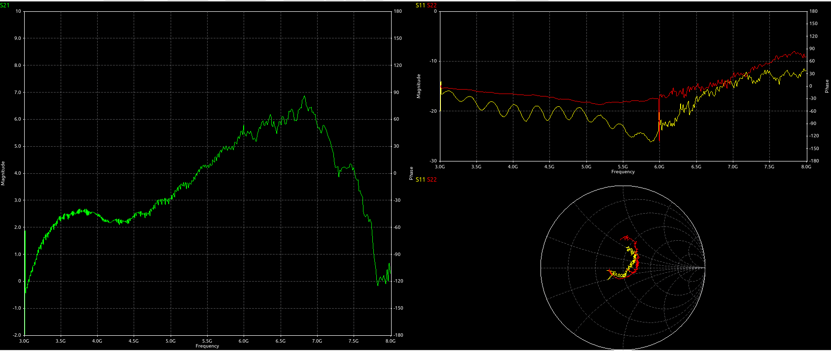
Output amplifier
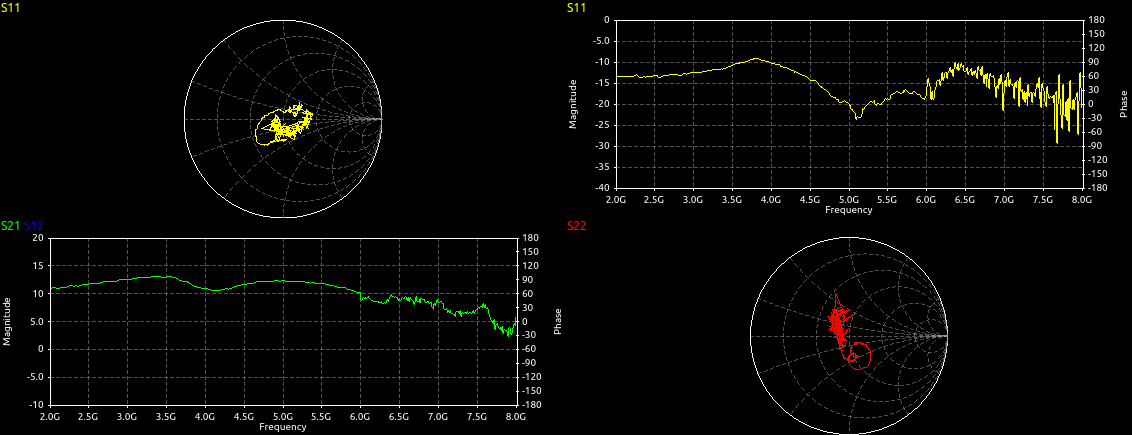
New amplifier was designed, measured and tuned.
Gain of 3 amplifiers connected (note: 2x 10dB attenuator installed – real gain is 22-27dB).
Output filter
Low pass output filter was removed because it probably didn’t work well (acc. my inaccurate measurements, too much loss at 7GHz and poor attenuation above).
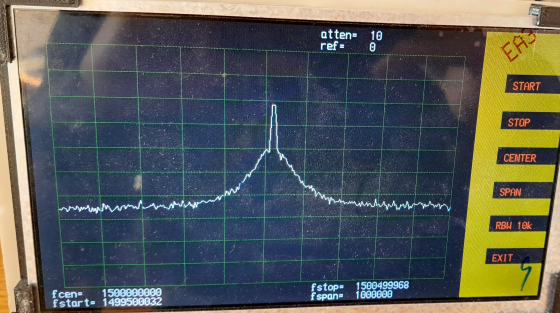
PLL
Improvements of PLL filter was important for phase noise. Initially, with both PLLs performing poorly I couldn’t get any results with RBW set to 1kHz.
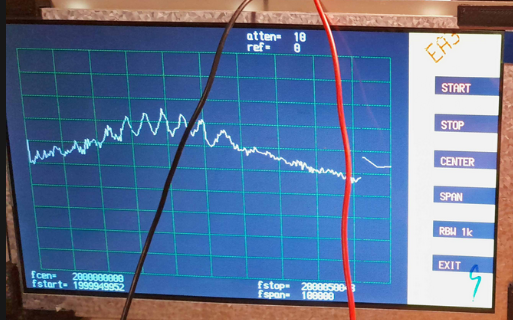
Dedicated software was used for the design, together with testing, trails errors.

With both filters for both PLLs (1st and 2nd LO) RBW 1kHz makes more sense. The filter removes a low of low frequency noise (which is large, especially in the prototype without any shielding)
Discussions
Become a Hackaday.io Member
Create an account to leave a comment. Already have an account? Log In.