I took a couple of PCB scans with the old setup using cheapo USB microscopes. I didn't include them, though. Why? Because the final image was noticably warped:

Again, the above is with a 12 dollar usb microscope, so you're not expecting it to be perfect --- but the warping makes it obvious that it came about by stitching. The same problem occurs to some degree with all objects, but is most apparent for rectangular ones. Usually I just crop them out strategically to provide a dishonest representation of how good they were to begin with.
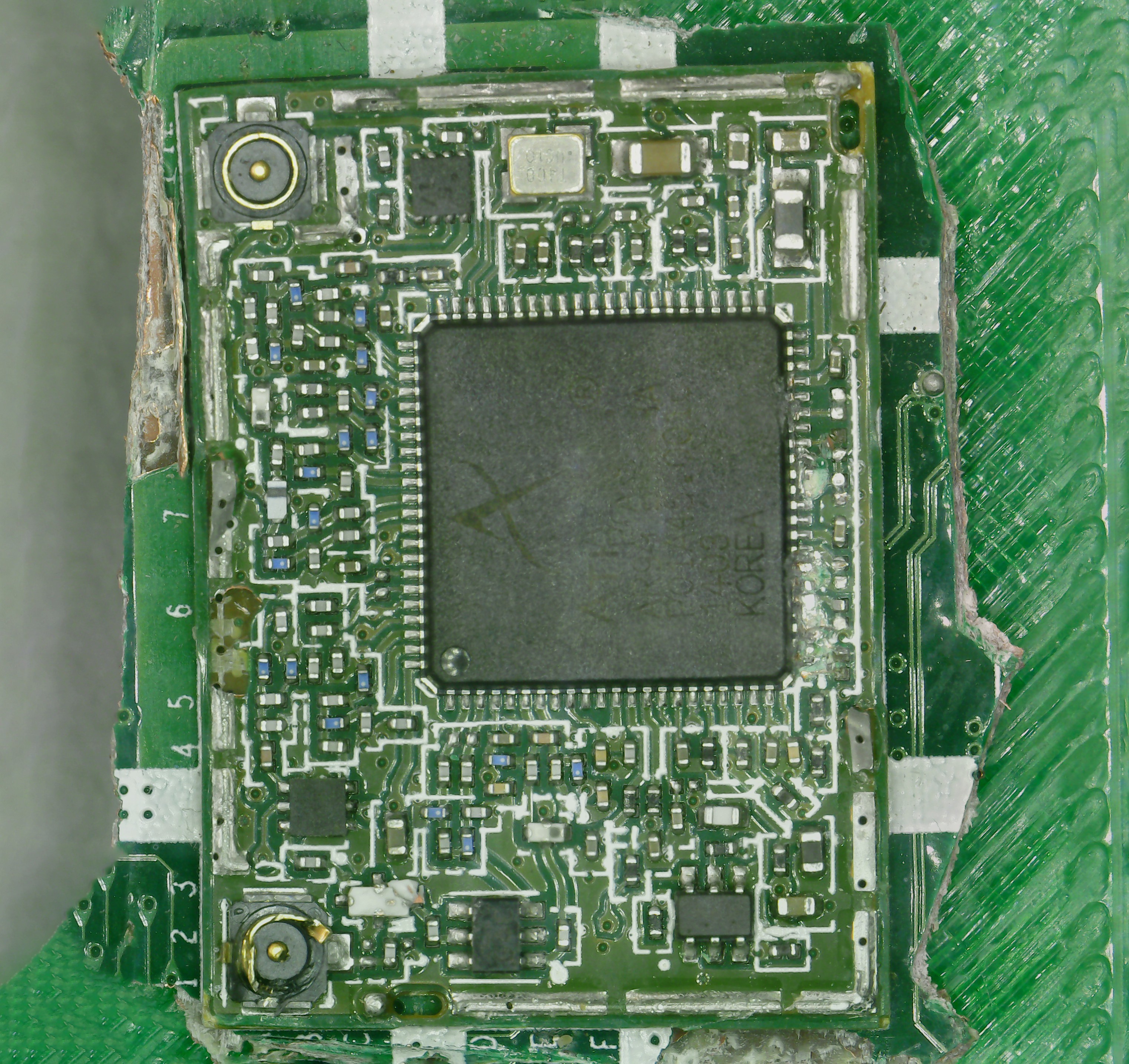
But the cause of the warping was a matter of debate --- how much was due to the 12 dollar camera and how much due to the software? A new scan sheds light on the problem:

Still not perfect, but quite noticeably better. 77 pictures with the scan itself taking 30 seconds. It turns out at least some of the warp is due to the camera, not the stitcher, even if you don't notice the warp on the individual pictures (I certainly don't). This also gives hope for some software solution if you can figure out exactly how much warp the camera is inducing and where.
That patch on the left side is where I pried up an onboard chip to provide a good area for a high res scan. I prepared it for a photogrammetry/photography superhero from facebook so he could try stacking with stitching for eventual 3D model generation efforts. Here is one set of 165 stitched pictures from a single Z height.

Decent stitch again, but with parts in and out of focus in the same frame (mixing and matching images isn't going to work the best here). That's why I took the same scan from 7 Z heights 0.1 mm apart, which enabled me to finally do something I've been meaning to for a while --- combine stacking and stitching. And it worked great!

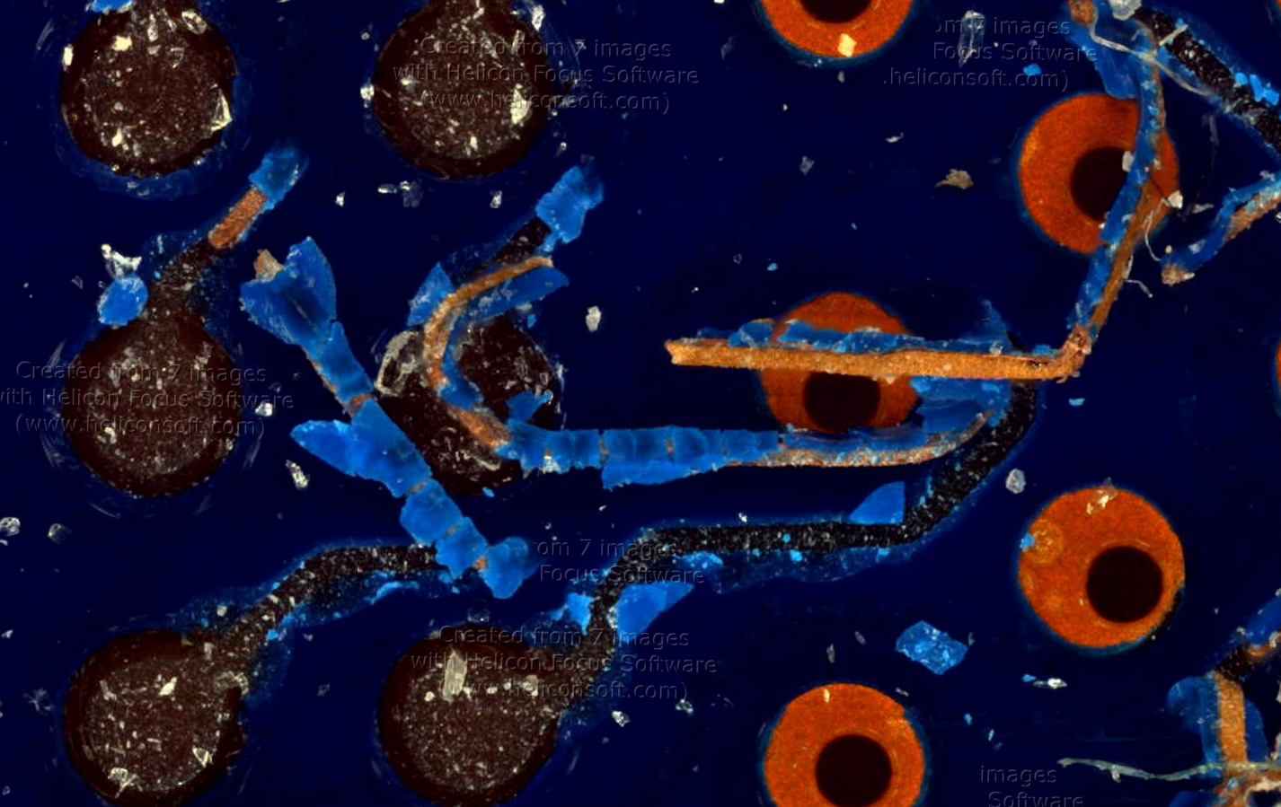
...until you look too closely and see, as with much of my work, the glue which holds it together:

I wonder which program I used the trial version of to do the stacking? Frankly I'm astonished that the watermarks didn't impact the the stitching process notably, like, at all.
I'd last like to add that theoretically, we have all the data now to create some kind of 3D rendering. Is it going to be 100 percent spot-on? No. Is it going to look decent enough? Perhaps. It depends on the application you are working with. The expert I consulted said that the programs demand accuracy to within a pixel, and would be seriously turned off by the x/y stitching process. In addition, expert was unable to "solve" the error profile for the lens used to take the pictures, which is part of the process in getting that sub-pixel accuracy. If you could solve the lens, maybe it would even improve the final quality of our cheapo 12 dollar microscopes.
So there's your PCB images. And I still have all the data from this scan, so I'm hoping that one day it will be turned into that 3D model after all. Stay tuned!
 Ahron Wayne
Discussions
Become a Hackaday.io Member
Create an account to leave a comment. Already have an account? Log In.