Close
0%
0%

IoT UPS

Small UPS with fix 3V3/1A output and adjustable 1.3 to 12V output, Li-Ion charger and protection

Similar projects worth following
The charger has been designed for IoT projects. The device uses very little current in "sleep" mode. During active mode 1A can be delivered.

Requirements

  1. Compact
  2. Powered by ubiquitous 18650 cells
  3. Option to connect Li-Po instead of 18650
  4. Including Li-Ion charger
  5. Charging while load is connected
  6. Charging options:
    1. USB
    2. 5V solar panel: up to 8V input should be accepted.
  7. Route VIN through : 5V output when powered by 5V
  8. Power input connector:
    1. USB micro
    2. JST-PH
  9. Outputs
    1. Primary output : 3V3/1A output
    2. Secondary output : 1.2V to 12V output, controlled by trimpot
  10. Efficient power conversion
  11. Low standby current
  12. Option to turn off outputs remotely to save power

COTS

Why make it when you can buy it?

  • TP4056, can be directly connected to solar charger
  • 3V3/1A created by 3 parallel LDO (77µA total quiescent current)
  • 5V/1.7A boost converter (260µA quiescent current).  There's no way to turn the boost converter off.
  • Not suitable to charge and discharge simultaneously.
  • Quite big

This one from AliExpress has only a 5V booster.

How much current is needed?

The original idea was to build a 3V3/2A supply.  But is that a good idea?  How many battery powered applications need a regulated 3V3 at 2A?  Sure we can build it, but it will be running at much lower currents for most of the times.  The efficiency at lower currents will be much lower.  The cost will be higher because of the bigger inductor and more expensive switcher.

1A will be enough for most applications, including the #easy-alarm-clock for which it has originally been designed.

Implementation

The original plan was to design a single PCB, but I expected to use this project too little.  Instead it will be converted to a modular design consisting of four small SMD-modules:

  1. Battery charger : will be existing TP5000 module (cheap, also charges LiFePO4, wide input voltage range)
  2. Battery management : existing modules based on the DW01A.  Wide range of current output ratings available (by paralleling FS8205A mosfets)
  3. Buck regulator based on AP3429A (obsolete?)
  4. Buck/boost (sepic) regulator based on LM2731X

BRD200110_R2.pdf

Schematic, PCB assembly drawing + BoM for version R2

Adobe Portable Document Format - 163.00 kB - 08/20/2020 at 09:30

Preview

Screenshot from 2020-02-03 20-51-50.png

PCB design

Portable Network Graphics (PNG) - 38.92 kB - 02/03/2020 at 19:53

Preview

  • Li-Ion battery level indicator

    Christoph Tack03/06/2022 at 07:18 0 comments

    We need a simple way to tell if the Li-Ion batter needs charging or not.

    "Precision" circuit

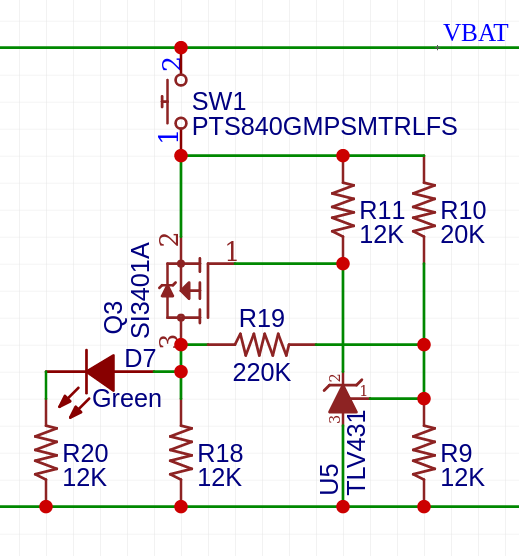
    When the switch is closed, the U5 will measure the battery voltage using the voltage divider R10/R9.  If the voltage on pin 1 of U5 exceeds 1.24V, then the cathode of U5 will be pulled low, causing Q3 to conduct.  When Q3 conducts, the LED D7 will turn on.

    R19 provides some hysteresis, preventing oscillation when the battery voltage is around 3.3V.

    R18 provides a drain path for the current when Q3 if off.  Otherwise, the current through R10 and R19 is enough to slightly turn D7 on.

    TLV431 as comparator with hysteresis

    The hysteresis voltage levels are 3.15V and 3.30V.

    The circuit is relative insensitive to component tolerances.  The drawback is that there's only one LED.  When the green LED is off, you don't know if the circuit is broken (but the battery is full) or when the battery is empty.

    Low cost circuit

    I came across the following circuit on the internet.  It exists in various variants, many even drawn incorrectly.  So it looks like some have trouble understanding how it works.

    circuits-diy.com/3-7v-lithium-battery-level-indicator-full-low/

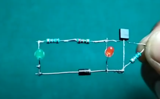
    The circuit works as follows.  When the battery voltage is low, the current will flow through the 1K+220ohm, the red LED and the 1K resistor across the BE-junction of the transistor.  The green LED will be off because the voltage over 1K+220ohm + the red LED, minus the voltage over the 1N4007 diode will be too small to turn the green LED off.
    Green LEDs typically have a higher forward voltage than red LEDs.  By adding the 1N4007 in series with the green LED further increases the needed voltage to turn the green LED on.

    As the battery voltage further rises, we'll reach the point where the voltage over the BE-junction will be enough to turn the transistor into conduction.  As the transistor conducts, the collector will be pulled low, causing the red LED be reverse polarized.  At that point, the red LED will turn off.  The battery voltage will now be sufficient to turn the green LED on.

    The values of the 1K+220ohm resistor is not critical because when the transistor is not conducting, the voltage at its collector will be the sum of the diode drop of the forward voltage of its BE-junction and the forward voltage of the red LED.  Both of which are relatively current independent.  Using a single 3K3-resistor works fine as well if that is what you happen to have laying around.

    I've built this circuit with a random green and red LED, two resistors (1K and 1K2), a 1N4148 diode and a BC847 transistor.

    • VIN > 3.0V ➭ green LED = ON
    • 1.6V < VIN < 3.7V ➭ red LED = ON

    The circuit has the advantage of having two LEDs.  The case where both are on at the same time also gives an idea of how much charge remains in the battery.

    Improved version of low-cost circuit

    Improvements:

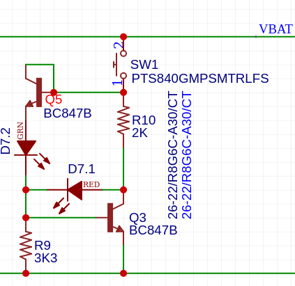
    • Reordering of LEDs allows for the use of bicolor-LEDs with common cathode.  I used a 1206-bicolor LED with two independent LEDs.
    • 1N4007 replaced by BC847B because it's already in the BoM.
    • R9 tuned to have the red/green transition at 3.3V.  You could place a 2K resistor here as well to shorten the BoM even more.

  • Power path management / diode OR-ing

    Christoph Tack02/14/2022 at 20:53 0 comments

    The problem

    During charging Li-Ion, the battery must be disconnected from its load, otherwise the charging algorithm won't work correctly.  At the same time, the load must still remain powered.

    The traditional solution

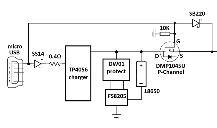
    As also shown in MCP7383X Li-Ion System Power Path Management Reference Design, the easiest solution is to use a diode, a resistor (10K in this case), and a PMOS.

    www.youtube.com/watch?v=T70mBHeIOZA

    The problem with this approach is the power loss and voltage drop over the diode.  Another problem is that the load may require periodical large currents that the USB-power supply can't handle.  Even if the battery holds enough charge to deliver that current peak, it's disconnected from the load.

    The sensible solution

    TI has solved the problem for us : bq2403x Single-Chip Charge and System Power-path Management IC and it includes a charger as well.

    The alternative solution

    Ideal diode circuits exist.  These "diodes" have a very small forward voltage, but typically a high leakage current.  So making them unsuitable for battery operation.

    The ideal diode solution : DIY

    Using COTS parts

    [Burgduino] used an LM66100 as ideal diode controller.  Unfortunately it only allows for 1.5A or so and it's a single-source solution.  To make matters worse, it's currently (Q1 2022) unobtainium.

    Alternative parts are the Torex XC8111AA01MR-G (unavailable March 2022), or the Analog Devices MAX40203ANS+T (unavailable March 2022).

    To handle larger currents, more of these parts would have to be put in parallel.

    Using discrete parts

    The ideal-diode problem is harder than it looks at first sight.  Consider we want to use two mosfets: one for the usb-path and one for the battery path.

    Either one of these mosfets should be on at any instant in time.  It's also allowed that both mosfets are off, but for a short period of time to limit heating in the internal diode.

    When does the battery-path mosfet need to turn off?  Before the usb voltage rises above the battery voltage.  Otherwise current from usb will drain away to the battery.

    When does the usb-path mosfet need to turn off?  Before the usb voltage drops below the battery voltage.  Otherwise battery current will drain away to the usb circuitry.

    A little bit of hysteresis generally improves stability on a comparator.  In this case, hysteresis should be limited because it causes the usb-path and the battery-path to conduct simultaneously.


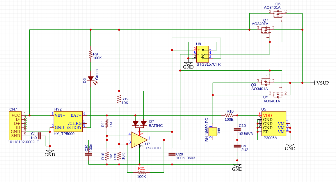
    U7 is a push-pull comparator which compares half of the battery voltage to half of the USB-voltage.

    The battery voltage is sampled using R11 and R18.  Because they're always draining the battery, they have a large resistance.  The high-impedance pin 4 of U7 becomes very susceptible to noise.  C30 effectively filters the noise on that node.
    The usb voltage is sampled with R19/R20.  These have a much lower resistance than R11/R18, to increase reaction speed to changes in usb-voltage. 
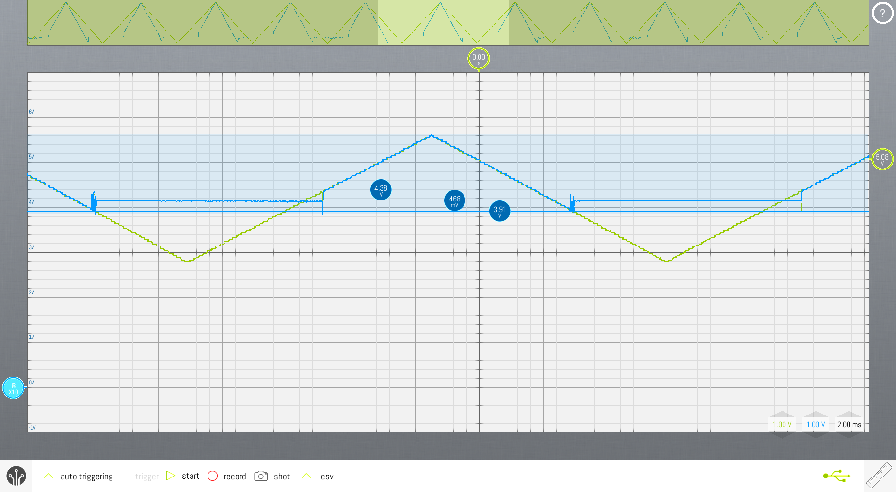
    R21 is the feed-forward resistor, causing a ±470mV hysteresis.  It might not be needed, but it's easier to leave it not-placed than to add it.

    The output of the comparator either switch Q3/Q5 ON or Q6/Q7.  You could use single mosfets if you need to switch lower currents.  Any 3401-mosfet will do.
    The 3157-analog switch is wired as an inverter.

    The 881-comparator, 3401-mosfet and 3157-analog switch are generic parts which can be sourced from multiple vendors.

    Additional components are a TP5000-charger module and a IP3005A battery protector.  These are single source 😢.

    GREEN = USB-voltage (taken a sawtooth here to clearly show hysteresis), BLUE = VSUP
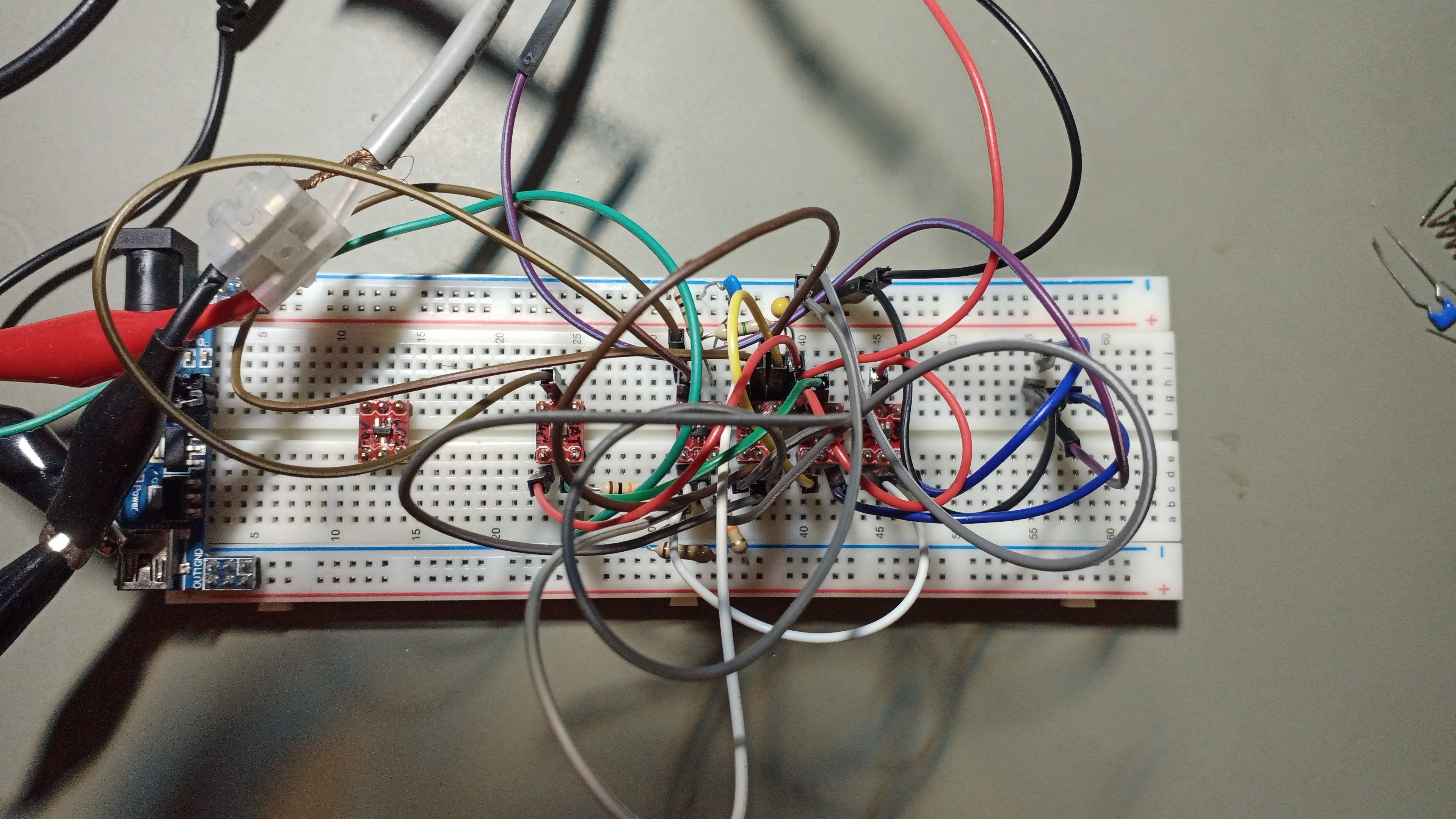
    Nothing better than a good nest of breadboard wires to verify your circuit.

    Test report

    TR_BRD200110R1.0

  • Testing R2

    Christoph Tack11/21/2021 at 16:51 0 comments

    Problem 1 : voltage drop on 3V3

    When the buck boost converter turns on, the output of the 3V3 converter drops by 200mV.  The problem is that the feedback resistors of the 3V3-converter are very close to one of the inductors of the SEPIC-converter.

    Swapping the location of the buck-converter and the SEPIC-converter as well as choosing 0603-resistors instead of 1206-resistors might solve the issue.

    Problem 2 : limited output current of SEPIC

    At an input voltage of 3.7V and the output voltage of 5V the SEPIC only reaches about 500mA.  Efficiency is also too low, reaching only about 60%.

  • Battery holder & PCB mounting

    Christoph Tack07/27/2020 at 19:53 0 comments

    It should be possible to mount the device easily.  There must be an option to connect two 18650 cells.

    MPD BH-18650-PC

    The battery holders below are through hole types.  The advantage is that it's easy to mount the PCB to a single or a dual battery holder.  These seem to be Chinese copies from the MPD BH-18650-PC battery holder.

    I think the battery holders below are designed for chargers, so that the battery can easily be removed.  There's no plastic on the side to keep the batteries in place.  The battery holders below might need a tie wrap to keep the batteries in place.  The MPD BK-18650-PC2 battery clip has been tested for shock and vibrations and is footprint compatible.

    Another disadvantage is that the through hole pins doesn't allow for the TP4056 module to be mounted on the edge of the PCB.

    Another disadvantage is that all components on the PCB need to be SMD types.

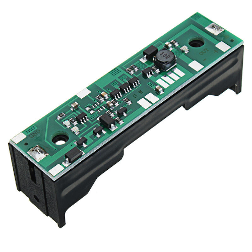
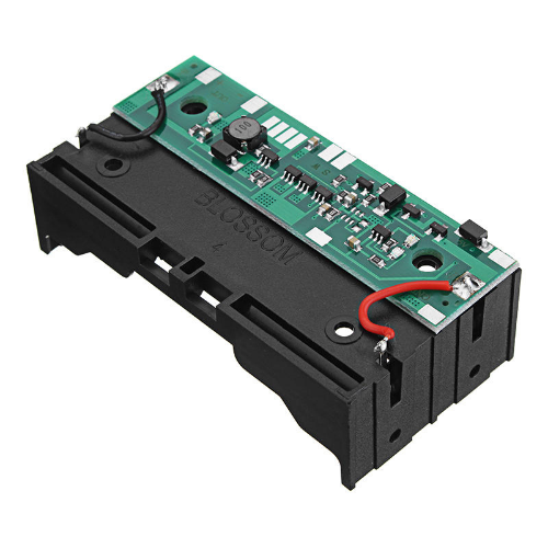
    12V UPS module from Banggood
    Simple way to connect a second 18650 cell

    Keystone 54

    Another option is to use the Keystone 54. It's an SMD type clip. Two are required per battery. They hold the battery firmly, but there's no plastic protecting the contact from accidental short circuits.

    Although the component is SMD, three through hole connections are required.  These make it impossible to mount the TP4056 module.

    Connecting a second 18650 battery can be done with a JST PH-header connected to the battery input of the TP4056.  The second PCB only needs the battery clips and the JST PH.  With a JST-PH to JST-PH cable, the batteries can then be connected in parallel.  There's more mechanical freedom to mount the batteries.

    Another advantage is that through hole connections can be made alongside the long edge of the PCB.  That might have been harder or even impossible with the through hole package.

  • DC-DC Conversion

    Christoph Tack07/27/2020 at 19:34 0 comments

    Buck, buck-boost / SEPIC or LDO?

    Buck-boost / SEPIC

    When looking at discharge curves from a Li Ion battery, it can be seen that at a battery voltage of 3V3, the battery holds only 15% of its original capacity.  There's little use in draining it further.

    LDO

    An LDO that can deliver 1A at 3V3 will be bigger, more expensive and will have a higher quiescent current than buck converter.

    I plan to use it when the 5V is connected for a longer period of time.  The Li Ion would only be a backup power supply.  In that case, an LDO is really a no-go because of its low efficiency at 5V input.

    Buck converter

    If currents >1A are desired,  this will be a more efficient solution.  Both energy and cost-wise.

    • AP3429A

    Input surge/reverse voltage protection

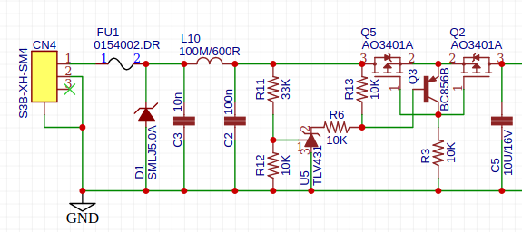
    This will consist of a fuse and a TVS-diode.

    An SMD-fuse holder, holding a standard 2410-size fuse will be used.  Littelfuse sells these as there OMNI-BLOK 154 series.  Chinese knock-offs can be found on AliExpress.

    The TVS-diode should be able to dissipate reverse current or over voltage until the fuse opens.  An SMC (DO214AB) package can hold 1500W or 3000W types.  So there's room for experiment.  The TVS-diode will keep the input voltage below 9.2V, so we must be sure that the battery charger and the buck converter can also handle this.  The AP3429 only accepts max. 6V, so we'll have to add extra safety measures.

  • Component choice

    Christoph Tack05/18/2020 at 18:57 0 comments

    Battery protection

    Mosfet

    DMG9926UDM

    Battery protection IC

    • AP9101CAK6-BVTRG1
      • UVLO = 2.8V (for uses where discharge currents > 3A)
      • over current detection : 100mV +/- 20mV
    • AP9101CAK6-ANTRG1
      • UVLO = 3.2V (for low power usage,)
      • Over current detection : 60mV (+21mV, -24mV from -40°C to +85°C)
    • FS312F-G : UVLO = 2.9V

  • Battery management

    Christoph Tack05/18/2020 at 18:42 0 comments

    Charger & protector selection

    A TP4056 charger & battery monitor module exists, but it takes up too much space.  So we'll implement it ourselves.  Some similar projects have been done:

    Charger

    The TP4056 has a big package.  Other charger IC's are available on digikey (MCP73831, bq21040, STC4054). 

    • The STC4054 has the highest leakage current when no power supply attached. 
    • The MCP73831 only accepts maximum 6V, while the TP4056 breaks at 8V input. 
    • The bq21040 seems the best deal.  It provides max. 800mA instead of the 1A on the TP4056.  It's 20 times more expensive than the TP4056, but it won't be killed by an input voltage up to 30V.

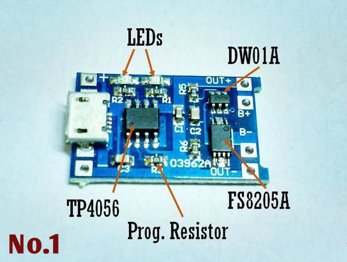
    TP4056 module

    • TP4056 module GREAT WALL Electronics Co., Ltd., €0.28
    • TP4056 datasheet
    • TP4056 Micro-USB Battery Charger Circuit Diagram
    • 1A charge current, set by R3
    • Implements charge termination, as continuously trickle charging a Li-Ion-cell should be avoided.
    • When VIN < Vbat, the module will only discharge the battery with a 3.7µA current.  3µA of it is due to the battery protection IC.
    • Battery protection IC.  The undervoltage lockout (UVLO) is an important parameter.  When discharging a Li Ion with a 1A or smaller current, the battery has already lost 90% of its energy when the battery voltage drops below 3.3V.
      • Fortune DW01A battery protection IC.  Alternative battery protection ICs such as the AP9101C also require about 3µA.
        • UVLO = 2.4V (Do not use this chip!), It's not recommended to discharge a  Li-Ion-cell so deep.
        • AP9101CAK6-family is pin compatible.
    • Contains dual NMOS
    • Automatic charge termination
    • Can be directly connected to a solar cell (#155 The 5 Best Solar ChargerBoards for Arduino and ESP8266)
    • pin 7: ON = charging (LED closest to USB connector)
    • pin 6: ON = charging finished
    Proposed setup in a device
    Proposed setup in a device

    A power switch (such as this PMOS) is needed because the LiPo can't be charged while being connected to the load.  The explanation lies in the charging algorithm.  Suppose the voltage of the LiPo has dropped below 3V3, then the TP4056 will only allow 60mA on its output.  If a load is connected that draws more than 60mA  there will be no current left to charge the LiPo.  The LiPo will remain discharged forever (or until the load is disconnected).  More info can be found here.

    The efficiency can be improved by replacing the schottky diode by an NMOS, switched by an NPN-transistor.  The base of the NPN-transistor is connected to 5V through a voltage divider.

    Battery protector

    Charging a battery is one thing, protecting it from over-, under voltage, over current is another thing.  The TP4056 module includes a DW01A protection IC and a double N-MOSFET: FS8205A.

    TP4056 module including battery protection

    More info about this module can be found here.

    The DW01A has a too low UVLO limit, so we'll replace it by the AP9101CAK6-ANTRG1.  The MOSFET's TSSOP8 package might not be so easy to solder.  The DMG9926UDM will be used instead.  You could also use the FS8205, which is actually the same as the FS8205A except for the package.

    The over-current protection can be set by using the AP9101Cxxx-ANTRG1 or the BV-variant.  A factor two in current increase can be gained by putting several MOSFETs in parallel as done here.

  • Design R2 : improvements over R1

    Christoph Tack05/10/2020 at 18:14 0 comments

    Power input connector

    The only allowed input voltage is 5VDC.  R1 had a JST-XH connector, which left a lot of room for erroneous connections: higher voltages than 5V and reverse power connection.  If we replace it with a micro-usb connector instead (Amphenol 10118192-0002LF), then it's clear for anyone how to connect it, where to connect it to and what supply voltage it's using.

    I don't like to see a micro-usb connector as a user interface connector because it's quite brittle.  Luckily Sparkfun has us covered here.  There's a Panel Mount USB-B to Micro-B Cable for $2.50.

    By using the micro-USB connector, we could leave out the reverse polarity, over voltage protection and over current protection.  The USB 5V power source will have these protections built in.

    Extra buck-boost converter

    This allows an extra output voltage, up to around 12V.

    Power output connectors

    The JST-XH connectors are too big for this small board.  They have been replaced by JST-PH.

  • Testing revision R1

    Christoph Tack05/01/2020 at 15:47 0 comments

    Over voltage protection section

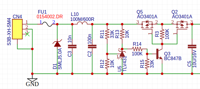
    The peak voltage over D1 is 9.2V, this would destroy U2.  To prevent this, an extra over voltage protection using U5 as voltage detection element and Q2 and Q5 as switching elements.

    Q2 and Q5 switch off when the input voltage rises higher than 5.28V.

    Applying 24VDC causes D1 to conduct, which trips the fuse FU1.  This is ok.

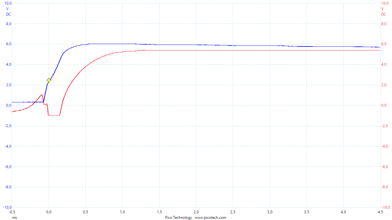
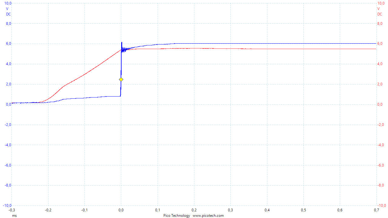
    To check if the circuit around Q2, Q5 works well, a voltage of 6.5V has been applied.  This is low enough to prevent D1 from conducting, but high enough to turn of Q5.

    Blue = voltage on C5. Red = voltage on gates of Q2 and Q5.  Notice that the red signal has a -100mV offset (I forgot to restore scope settings to default).

    There's clearly something wrong with this design.  Low voltage turn-on is quick due to U5 that starts conducting, but turn off of Q2 and Q5 is too slow.  This results in the voltage on C5 rising above the designated 5.28V.

    Decreasing R3 will speed up the discharge, but this design is inherently flawed.  Turning of Q2 and Q5 should be lightning fast to prevent damage to U6.

    Solving the problem

    Small rearrangement solves the problem
    The input voltage is 6V.  As the threshold of 5.3V is reached, the gate voltage of Q2 and Q5 rises fast, which turns them off quickly.  As a result the voltage on C5 doesn't rise above the 5.3V.
    Blue = voltage on gates of Q2 and Q5, Red = voltage on C5

    Charging section

    Charge current is set to KISET / RISET = 540 / 1K = 540mA.

    The Li-Ion cells I used were at the end of their lifespan, but they Initial constant current charging happens at 430mA.

    The red LED is on during charging.  After the charging process is completed, the LED turns off;


    Lithium Ion protection section

    After insertion of a Lithium Ion battery, briefly connect it to the charger.  This is needed to take the protection-IC out of Power-Down mode.

    Although I ordered the AP9101CAK6-ANTRG1 from Digikey, the auto-wake-up functionality, designated by the A, doesn't work.  After battery insertion, charger connection is needed.

    Over voltage

    • Measured : 4.25V
    • Datasheet AP9101Cxxx-ANTRG1 : 4.225V

    In case of over voltages, the CO-pin will go low.  Remark that this doesn't fully disconnect the battery from the load.  Discharging the battery is still possible.  A load connected to the battery will still be able to draw current from the battery.  The current will flow through the channel of the FET controlled by the DO-pin.  This FET is still conducting.  The current then follows its path through the body diode of the other FET, which is off.

    This is a useful feature, as it allows the battery to return to a safer state.

    In case of over voltage (most likely to be caused by over charging), when CO-pin is low, charging is no longer possible.

    Under voltage

    • Measured : 3.22V
    • Datasheet AP9101Cxxx-ANTRG1 : 3.20V

    In case of an under-voltage-event, the DO-pin will go low.

    Over charge current

    todo

    Over discharge current

    The circuitry has been connected to an electronic load.  Using the DMG9926UDM-7, the maximum current was 1.35A.  This is mainly because the AP9101Cxxx-ANTRG1 has a VDOC of only 60mV.  Replacing the battery protection IC by the BV-variant, would increase the maximum discharge current to 2.25A.


    3V3 buck regulator

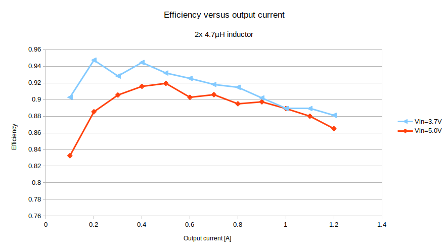
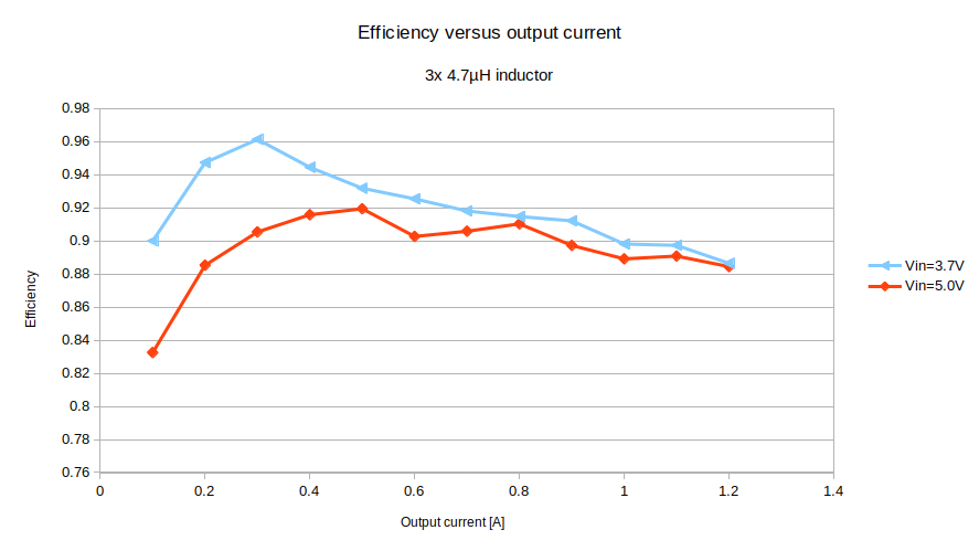
    Efficiency measurement

    An electronic load has been used as load on the 3V3.  The board was powered using the thin wires from the JST-XH leads.

    Efficiency for powering the buck with 3.7V (Li-Ion) or 5V (USB) and two parallel inductors in the SMPS.

    Efficiency for powering the buck with 3.7V (Li-Ion) or 5V (USB) and three parallel inductors in the SMPS.

    Remark that if we had used an LDO instead of this buck regulator, we would have had 90% efficiency (theoretical maximum) for 3.7V input and only 66% efficiency (theoretical maximum) for 5.0V input.

    Ripple measurement

    For that we apply a...

    Read more »

View all 9 project logs

Enjoy this project?

Share

Discussions

ShirleyClinton wrote 08/29/2023 at 08:39 point

This is really useful information i must say that this is really nice thanks for sharing with us. https://www.adpworkforce-now.com/

  Are you sure? yes | no

Similar Projects

Does this project spark your interest?

Become a member to follow this project and never miss any updates