 Yann Guidon / YGDES
So one latch "building block" is this :
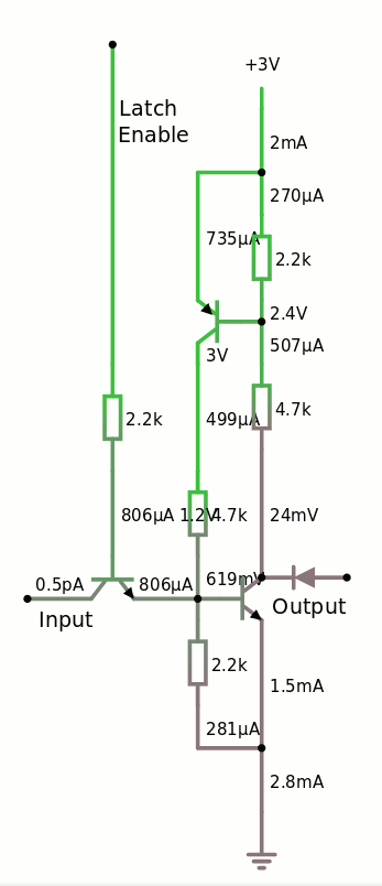
BOM:
- 1 PNP
- 2 NPN
- 1 diode for the output (might be removed in certain cases, such as when driving another base)
- 3× 2K2
- 2× 4K7 (could be 2× 2K2 if needed)
A "slice" is a "DFF and a half" : one master latch and two slaves, one of them can be connected to the processor.
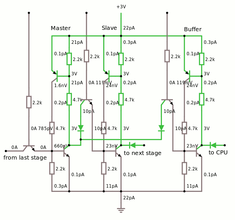
This is pretty easy to place & route on a small board.
In this example, the "slice" is configured for the receive circuit (SIPO). The 3 latches must be connected differently to perform the PISO function, so each "slice board" would have each individual latch connected to the outside so a backplane can configure the correct function.
Discussions
Become a Hackaday.io Member
Create an account to leave a comment. Already have an account? Log In.