 Tim
Tim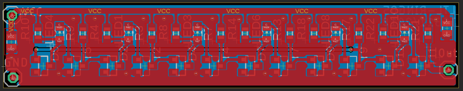
After characterizing a basic NAND2 gate, the next step is to measure the timing properties of the LTL gate. For this purpose I built a ring oscillator based on five gates. The PCB design is shown above. I added one additional inverter as an output buffer to avoid loading of the oscillator while measuring its frequency.
I built two versions of the ring oscillator: One with red LED and one with green LED, both using 1.8k collector resistors.
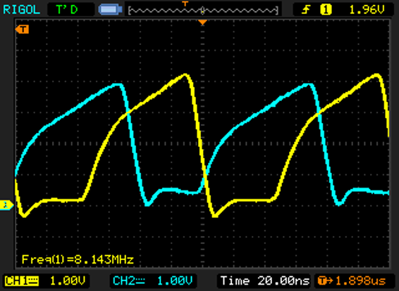 The scope screenshot shows the input (yellow) and output (turquoise) waveform of one inverter in the ring oscillator (green led). The falling edge is steep since it is actively pulled down by the transistor. The rising edge is, again, separated into two regions depending on wether only collector resistor or base and collector resistor are involved in pulling up the node.
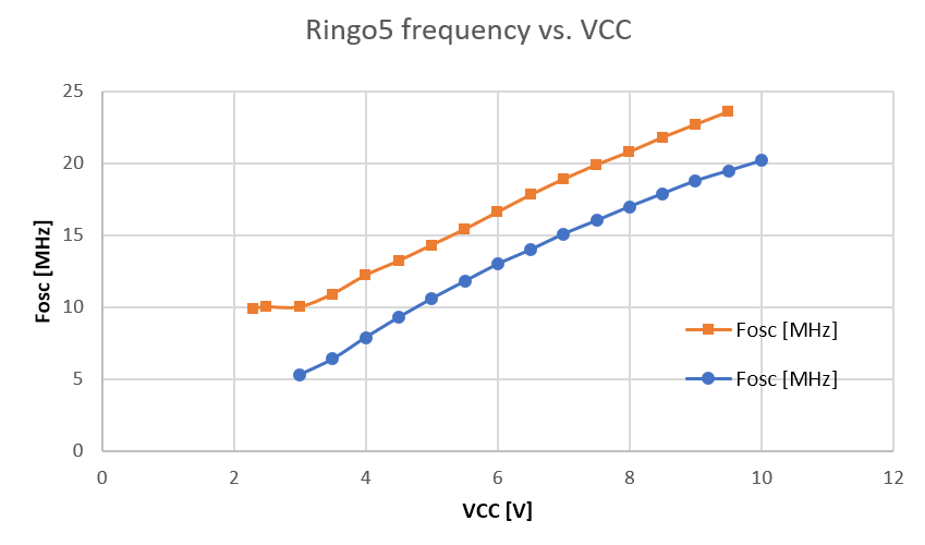
The diagram above shows measurements of ring oscillator frequencies versus supply voltages. The blue line corresponds to the inverter with green LED, the orange line to a red LED. There is a clear trend towards higher frequency for higher supply, which can be explained by the availability of more switching current. The red LED LTL gate has a lower threshold voltage and does therefore switch earlier and faster. Since this design is based on the PMBT2369 switching transistors, no dominant influence of base saturation is observered. LTL gates with normal small signal transistores should exhibit a speed-supply relationship similar to what I observed with RTL.
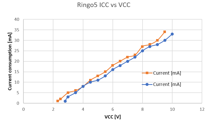 The supply current shows a linear relationship with supply voltage, as expected for a resistor-loaded gate.
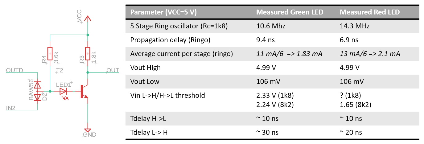 The table above summarizes the charactization of the LTL gates. There is a tradeoff between high noise margin (green LED) and speed (red LED). All in all, the propagation delay looks very acceptable for discrete logic. At tp=6.9ns, the red LTL gate is almost as fast as the RTL gate in a CDC6600 and still much faster than the BC847 based DTL gates used in the MT-15, while maintaining full 5V CMOS/TTL logic level compatibility.
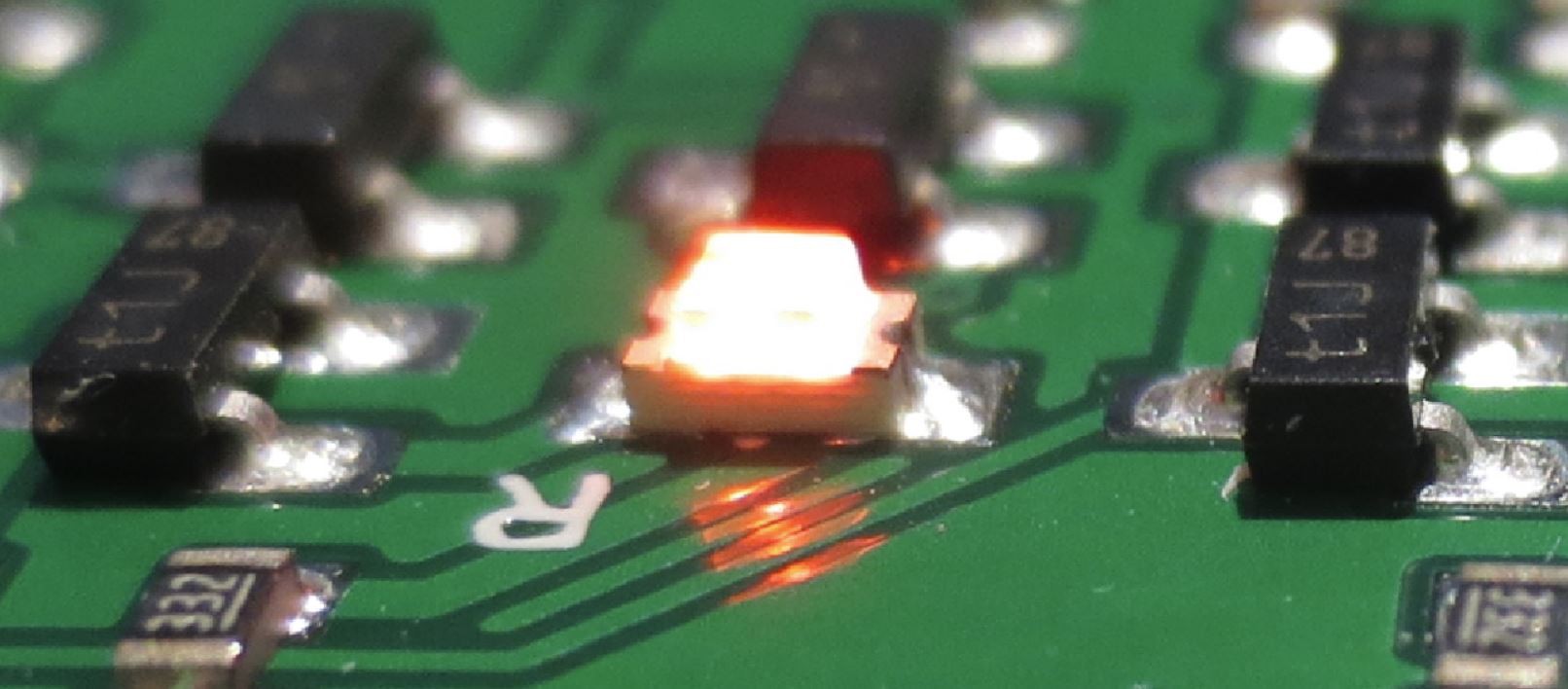
Did I mention that each gate comes with its own blinkenlight?
Discussions
Become a Hackaday.io Member
Create an account to leave a comment. Already have an account? Log In.