 Tim
TimNow to the last category of building blocks: Flip Flips.
If you grew up learning about digital electronics in the advanced CMOS era, like me, you will most likely be accustomed to using edge triggered flip flops for everything. Unfortunately, it turns out that proper edge triggered flip flop require at least 6 NAND gate equivalents, unless you have dynamic CMOS logic at your disposal.
For those of us who were suddenly beamed into the discrete LTL age, latches are a much more part count efficient solution, as they only consume about half as many components as a static edge triggered flip flop.
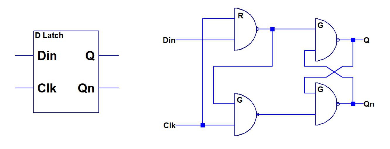
A commonly known minimal representation of a gated D-latch in NAND2 is shown above. See also Wikipedia article. A nice propery of this design is that it only requires a single clock input and has both inverted and non-inverted data outputs. Data from Din is forwarded to the output while Clk is high. The state of the latch is frozen on the high->low transition of the clk and held while clk is low.
When using this design in high speed circuits it becomes apparent that it has a nasty habit of generating glitches. The origin of this effect is the NAND2 gate in the lower left. The clock signal arrives on one input directly and on the other it is delayed through the NAND2 gate in the top left.
This effect can be somewhat reduced by tweaking the propagation delay of the logic gates. In LTL this is easily possible by changing the LED color to change threshold voltage. In this case I introduced a faster "red" (hence the R) gate with lower threshold as the top left gate.
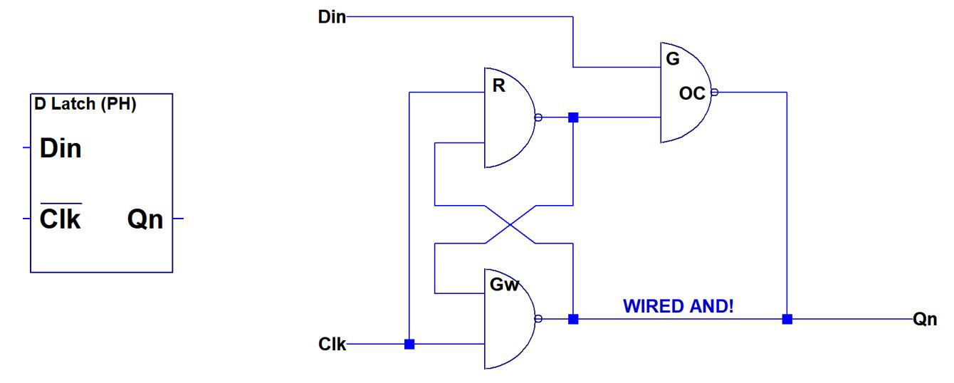 There is also a way to reduce gate count to three by replacing one of the NAND2 gates with a wired AND. This is described in a now expired patent. (A similar design is described in this patent)
The patent also describes to work around the aforementioned glitch by introducing one faster gate. A disadvantage of this design is that it is only has an inverted output. The clock input is also inverted compared to the previous design: Data will be forwarded for clk='0' and held for clk='1'.
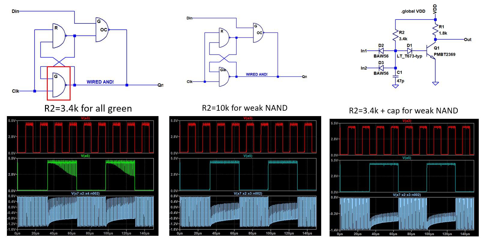 One very important point of learning came out of actually simulating a full design including the latch and observing dynamic operation. To do this, it is necessary to perform a transient simulation in Spice - LTspice was used here.
 The figure above shows simulation results and modifications to the latch design that were applied as a result of the observations. The latch was used as part of a program counter here. The first line (in red) of the simulation traces shows the fourth bit (A3), the second line shows the sixth bit (A5).
The leftmost column shows the results of the unmodified circuit. A3 looks nice and clean. However, A5 shows a series of negative spikes when the output is high. Interestingly, this behavior changes over time. It should be noted that this is mostly a cosmetic issue at this point, because the glitches are far away from the clock edge were the data is latched. Elminitating this effect should still be a priority as the additional noise may snowball into actual bit errors when the timing gets more tight.
The culprit is the gate indicated by the red box, which receives a clock signal that is partially delayed by another gate. The lowermost trace shows the node directly at the base of the gates transistors. This node is basically floating when the gate is turned off, since both the LED and the base junction are reverse biased. You can see that it assumes a deeply negative potential. It appears that some of the charge on the node trickles away over time, making the gate more sensitive to spikes on the inputs.
A solution to this issue is to make the gate in question "weaker", so it becomes less sensitive to transient conditionts at the inputs. I tried two ways of doing so: Increasing the base resistor (middle column) and by adding a small capacitor (right column). Ultimately I settled on the additional capacitor, because increasing the base resistor would reduce the current through the LED which makes the LED Vf unpredictable and reduces blinkyness (important!).
A case in point: Don't underestimate the trouble with latches. I settled on the design above for now, but would most likely look into further options when starting another design with LTL.
Discussions
Become a Hackaday.io Member
Create an account to leave a comment. Already have an account? Log In.
Interesting !
The amount of ringing, when the clock is enabled, is staggering and totally unsuitable for a conventional circuit (unless I missed some critical insight).
I tried to simulate at the logic level and there is indeed a lot that can go wrong. One example that is not too bad is :
http://www.falstad.com/circuit/circuitjs.html?cct=$+1+0.000005+0.8031194996067259+50+5+43%0A151+256+384+336+384+0+2+5+5%0A151+128+192+208+192+0+2+5+5%0A151+128+368+208+368+0+2+5+5%0Aw+128+384+96+384+0%0Aw+128+352+128+304+0%0Aw+128+304+208+272+0%0Aw+256+192+208+192+0%0Aw+128+208+128+272+0%0Aw+128+272+208+304+0%0Aw+208+368+256+368+0%0Aw+336+384+336+304+0%0Aw+336+304+208+304+0%0AL+96+384+48+384+0+0+false+5+0%0AL+240+400+240+432+0+0+false+5+0%0Aw+96+384+96+176+0%0Aw+96+176+128+176+0%0AM+336+384+384+384+0+2.5%0AM+336+208+384+208+0+2.5%0Aw+256+400+240+400+0%0Aw+240+400+240+224+0%0Aw+240+224+256+224+0%0Aw+208+272+336+272+0%0Aw+336+272+336+208+0%0A152+256+208+336+208+0+2+5+5%0Ao+4+1+0+4230+5+0.1+0+2+4+3%0Ao+10+1+0+4230+5+0.1+0+2+10+3%0Ao+3+1+0+4230+0.0000762939453125+0.1+0+2+3+3%0A
Anyway, feeding the clk signal to both inputs of the interlocked NAND2 necessarily results in oscillation/metastability, it's a logic issue and not an analog domain trick.
I'm looking forward to seeing your own sim & circuit in Falstad and be proved wrong :-)
And yes, the MUX-based latch is much safer.
Are you sure? yes | no
This typie of latch only works with real parasitics. To stabilize it, it is necessary to modify thresholds of the gates to create intentional delay skew. Also, the slew rate of the clock needs to be finite.
It's discribed above and also in this patent:
https://patents.google.com/patent/EP0092663A2/en
Falstat will not be able to simulate this with pure boolean logic gates. But it works in Spice and in real hardware.
Are you sure? yes | no
to me, it's still like playing with fire ;-)
Are you sure? yes | no
Somehow your circuit looked quite different from the original. I came up with the one below. It does still not work, and the reason is probably because falstad uses purely digital signals. The additional AND gate in the latch-feedback adds one cycles of simulation delay, which results in an oscillating behavior of the latch. That is obviously not realistic
http://www.falstad.com/circuit/circuitjs.html?ctz=CQAgjCAMB0l3BWKsAsCDMkAcBOSYB2AJi3wDYcQFIqQV0AoMBCIhM8Aj9dDwjmkVoImLcCXA4hRbJKGCoVURDATeWEDI3rF8pQHdx2rChA5uJqA0OqNWo5uJWbEok-uZTkayHQIhPNz+mrLeADJmFqYoxl7gIABmAIYANgDOAKa04ZEOMQ40NMnpWUjehua+lpX8zrm1tpwCDACydKS+wf7awYLQIoYxNH5CKPkjdUREpo3TNI3lmuzgZIIo86uT6ytr8xKLUzMSNfs+Ex7BtYsTtYFNdUO+kKYezw8dnu3DvWfBd+iWO7eZjDQHBMY9PRCJADEIaMBSTTbBHyHxzORIwTLA7IxFsPiInFYjjotyowyk9yyMmTalORqfRYMt4Mn4U2Q6dE6Im+MixXkabwAexAfEUKCImGy0AgCm4DBF6HiNAlUrKMt0vl8CvAKnFkBwGnVerADCAA
Are you sure? yes | no