 Tim
TimDesigning the control unit is one of the more complex tasks in MCU design. What used to be a few lines of VHDL turns out to be a tedious task when boiling it down to discrete gates. Or maybe I need a better design flow...
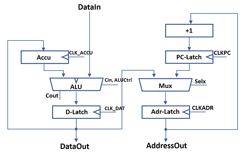
Lets look at the problem at hand. The final LCPU will consist of an 8 Bit datapath and an 8 Bit adresspath. The upper two bits of the addresspath will be used for the opcode. Since both the data and the ALU board are 4 bits wide, two of each ports have to be used.
To complete the CPU, we need a control unit that outpus the right control signals in depends of opcode and state machine cycle.
The original MCPU has a rather simple control unit that consists of a state machine that is directly mapped to opcodes. Decoding of the states is localized at the datapath. Since the LCPU uses a bitslice approach, it is more efficient to also include decoding of states into control signal in a centralized control unit. Generally, that is a design choice that allows for extending of the design and easier bugfixing. In terms of robustness it would be better to do localized state decoding to reduce the number of control signals.
There are 8 ALU board control inputs (Carry In, CLK_ACCU, CLK_DAT, Aluctrl[4:0]) and one output (Carry Out). The address board has 4 control inputs (SEL_PC, SEL_DATA, nCLK_PC, nCLK_ADR) and two outputs (OPC1,OPC0 -> A[7:6].
The control board itself has a few internal registes for carry and states and inputs for a two phase clock (phi1,phi2) and reset.
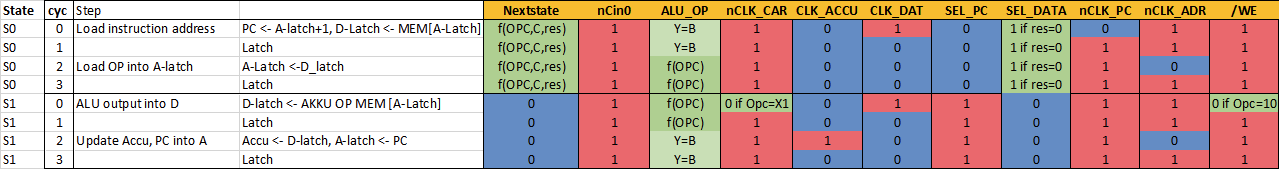
As a first step, I mapped all control signals to states and clock sub-cycles. The LCPU is still able to execute every instruction in a maximum of two clockcycles, despite switching from edge-triggered FF to latches.
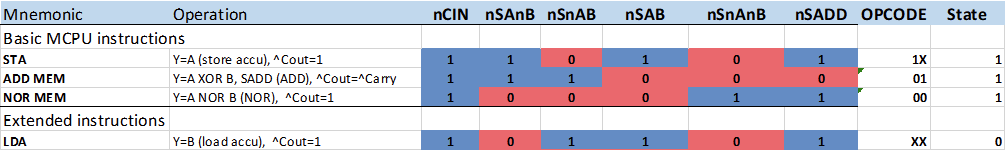
ALU control signal encoding in dependence of Opcode and state.
 Many of the simpler control signal encodings could be directly mapped to single gates. In additional you can find three latches for Carry signal and state enconding here, in what could best be described as "sea of gates". Very tedious to layout on the PCB, but straightforward in implementation by using the building blocks I designed earlier.
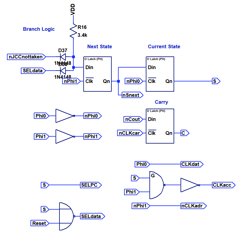 Of much more interest is the AND-OR-INVERT logic array that is used to decode the more complex signals, specifically the opcode into ALU control signals. You can see the circuit below.
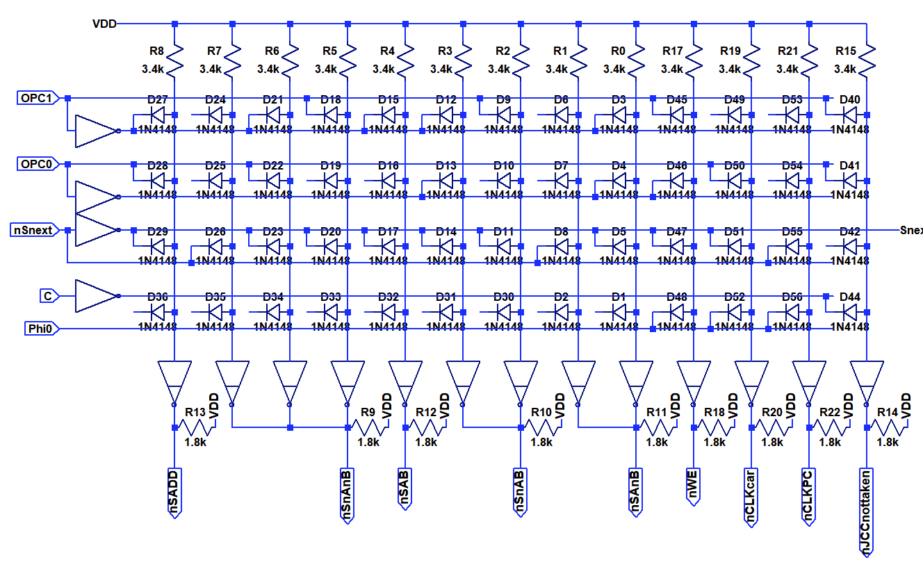 Instead of using double diodes I switched to single diodes to allow layout in a regular matrix. Input signals are routed vertically on the rear side, output terms vertically on the front side. Typically both the inverted and non-inverted inputs signals are provided by means of the inverters on the left side. Each column represents a multiple input AND-gate (Minterm). By connecting the diodes not at all or to the positive or negative input signal it is possible to crate any convolution of AND-operation. The opon collecter inverters at the bottom perform a "NOR" operation on any number of input terms. By combining these, it is possible to implement any boolean operation with only minimal changes in the layout. I decided to populate also unused diodes in the matrix to allow for later fixability.
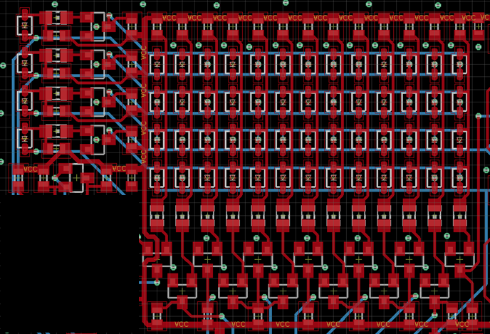
The full layout of the logic array is shown above. As you can see, the schematic represents the arrangement of the layout quite well. The density is quite good, the full layout is just 45x33mm². Even though the array itself does not use LEDs, the input and output inverters are true LTL gates, so that blinkyness is garuanteed!
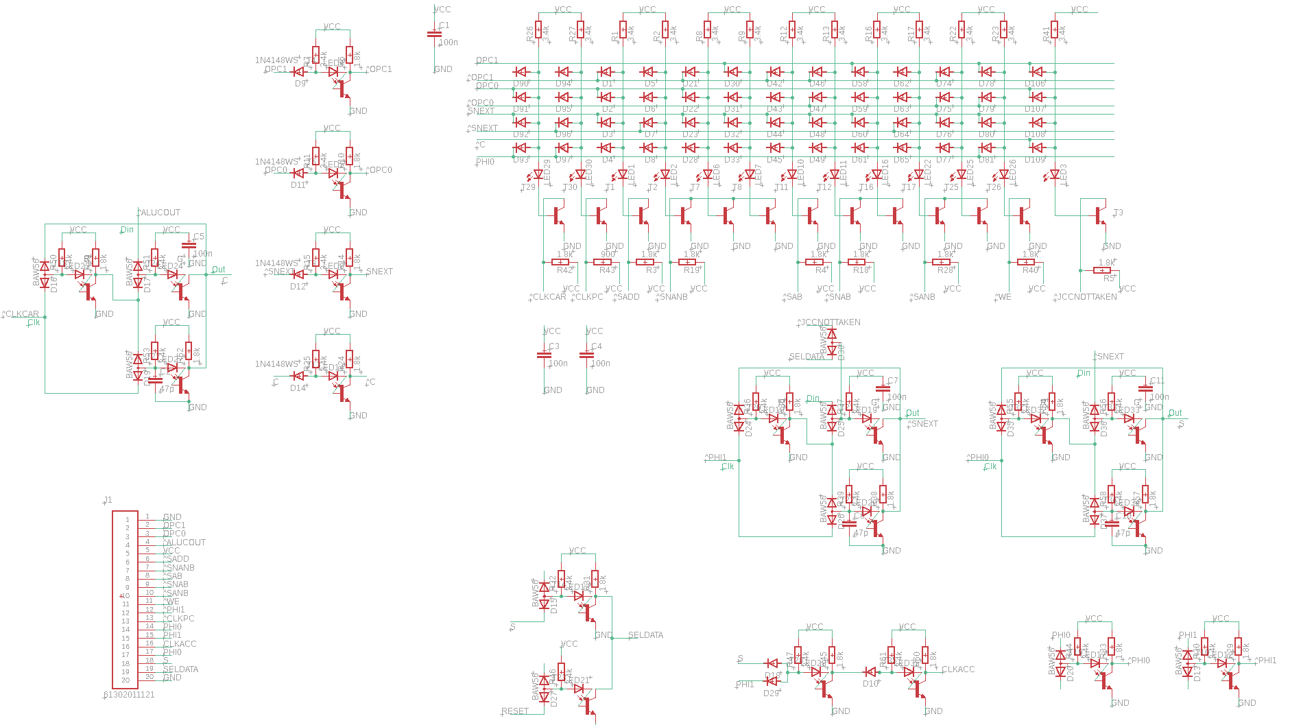 For the sake of completness, the full schematics for the board level implementation are shown above.
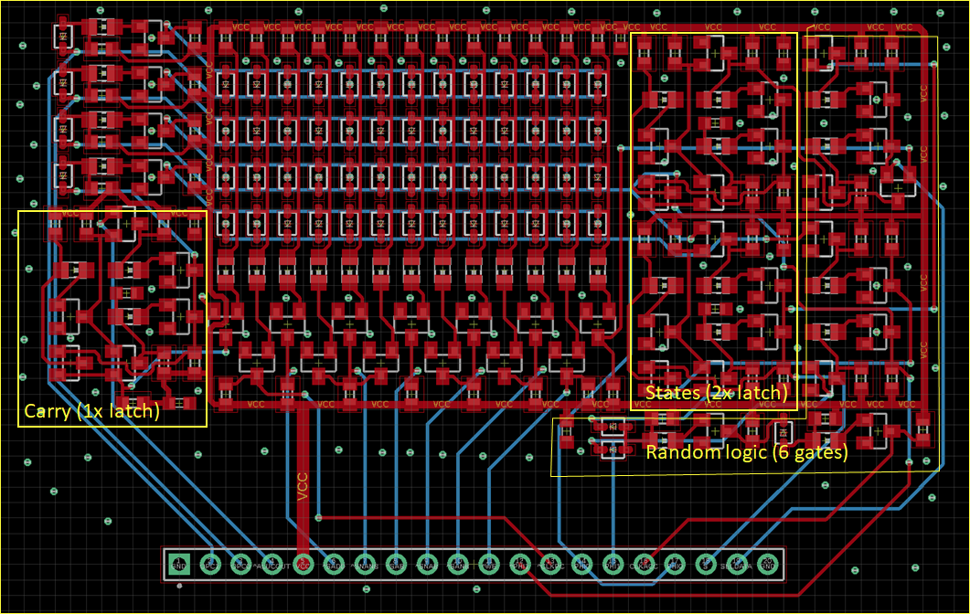
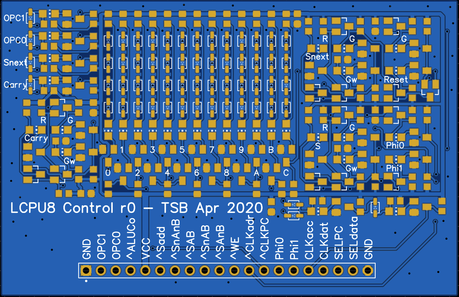
You can see the full board with a few annotations above. (This feels like annotating an IC...). Total size is 78x50mm². Off to manufacturing...
Discussions
Become a Hackaday.io Member
Create an account to leave a comment. Already have an account? Log In.