 Jeff Cooper
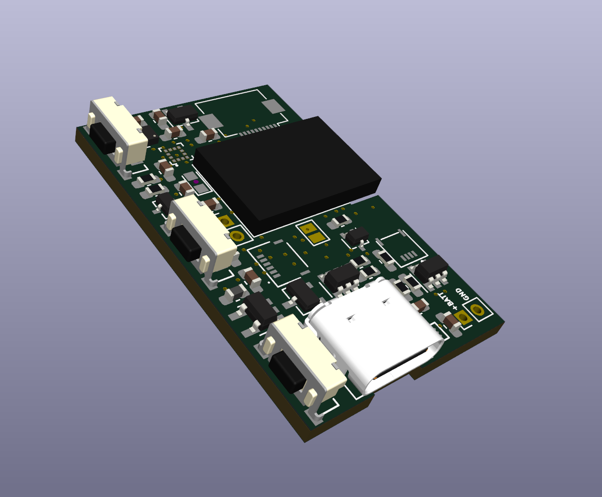
Small update tonight: I just finished routing the rev. 5 PCB for the watch, which has a few small but notable improvements:
- A TVS diode array protecting the USB power and data lines. After a pile of clean laundry killed a voltage regulator last night, I had the realization that most, if not all, of my inexplicable power system failures could be explained by ESD events. Hopefully, rev. 5 won't have that problem.
- Instead of hard-wiring the enable pin on the 5V boost converter that drives the display, it's not controlled by the MCU. I also added a schottkey diode pair that drives the display with the higher of VIN (the battery) and +5V (the regulator). Experimentation shows that the display will function fine until the mid-3-volts range, and the 5V boost converter draws 90uA quiescent while enabled. As long as the battery has a voltage that the display is happy with, I can now shut off the boost converter and save those 90uA. This does mean, somewhat amusingly, that I'll actually have to increase the power draw (by turning on the boost converter) when the battery gets low.
- In rev. 4, I had broken out through-hole connectors for VUSB, D+, D-, and GND, in the hopes of later adding some sort of dock. Those holes got in the way, so in rev. 5 I overlaid the USB connector with an FFC connector that could be soldered instead. When I do get around to building a dock, I should be able to remove the USB connector and use an FFC connector to connect to the docking hardware instead. In the meantime, the USB port remains fully functional.
- I replaced the board-to-board AXT[5,6]10124 connector pair (intended for a flexible circuit board holding the flashlight and wrist-side buttons) with a 6-position FFC connector. Rather than having to wait 3+ weeks to iterate on flexible PCBs for the wrist-side daughterboard, I decided to instead use a short FFC cable to connect to a low-profile rigid circuit board on the wrist side. This may end up adding a fraction of a millimeter to the wrist side of the watch, but the ease of assembly and iteration should more than make up for it. I also found some interesting low-power capacitive sensing options for the wrist-side that I might try. Rather than GPIOs, I broke out the I2C bus and a single GPIO for interrupts. This should give me more options to experiment if my initial ideas don't pan out. (I did consider that I can use two GPIOs as a second I2C bus, but I thought that enabling a second I2C peripheral might draw more power than I need. There are low-power I2C GPIO expanders if I need them).
- I removed the reset button and replaced it with a jumper. I didn't even bother soldering the reset button on the rev.4 board, so I figured I could reclaim the board space and short the jumper with a wire in the rare case that I need to do a hardware reset -- most of the time I use software resets, and my firmware enables the watchdog timer to reset itself after a few minutes in case it gets hard stuck.
I also did a tiny bit of software work to move towards having a real interface. This involved shuffling around a bunch of source files to make PlatformIO's build system happy, but otherwise there's not much to report.
The next few updates will probably be software, since I'll probably get daughterboard and dock prototype board finished tomorrow and sent out for fab over the weekend, then I'll have to wait a week or two before I can start assembling and testing.
Discussions
Become a Hackaday.io Member
Create an account to leave a comment. Already have an account? Log In.