 land-boards.com
Did quite a few changes to the VHDL code. Here it is in GitHub.
- Added vma (Valid memory address) signal into write strobes
- Made CPU clock run at 1 MHz (will probably run faster)
- Removed ACIA code - just using VDU with 6850 interface
- Moved ACIA base address to $8018-$C8019 (Matches Smithbug v2)
- Gating clock (not) into write strobes
- Re-named signal names generally per Nandland signal naming conventions
- Left External SRAM and SDRAM interfaces but drove to inactive levels
- 4KB of EPROM with 4X "copies"
- 32KB of SRAM
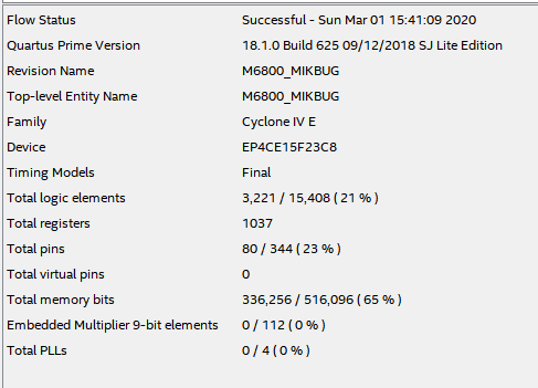
- Fits into FPGA with room to spare
Discussions
Become a Hackaday.io Member
Create an account to leave a comment. Already have an account? Log In.